Substrate transfer system and transfer method

A transfer system and substrate technology, applied in the direction of electrical components, printed circuit manufacturing, electrical components, etc., can solve the problems that cannot meet the needs of production, achieve the effect of improving efficiency, long improvement cycle, and satisfying the improvement

Inactive Publication Date: 2010-01-20
AVARY HLDG (SHENZHEN) CO LTD +1
View PDF0 Cites 10 Cited by
  • Summary
  • Abstract
  • Description
  • Claims
  • Application Information

AI Technical Summary

Problems solved by technology

However, with the improvement of the speed of each process of circuit board production, this kind of retractable device cannot meet the needs of production.

Method used


Image

  • Substrate transfer system and transfer method
  • Substrate transfer system and transfer method
  • Substrate transfer system and transfer method

Examples


Embodiment Construction

[0012] The technical solutions provided by this technical solution will be further described in detail below in conjunction with the accompanying drawings.

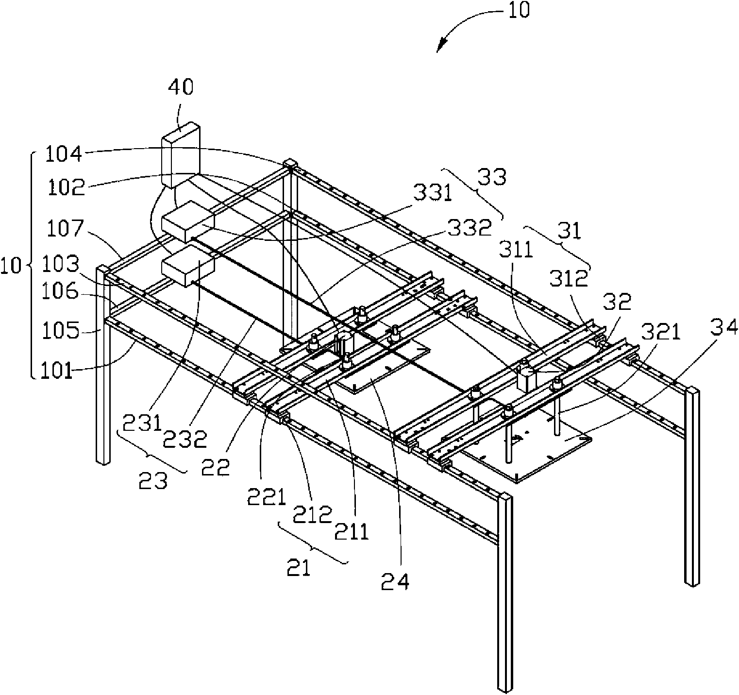
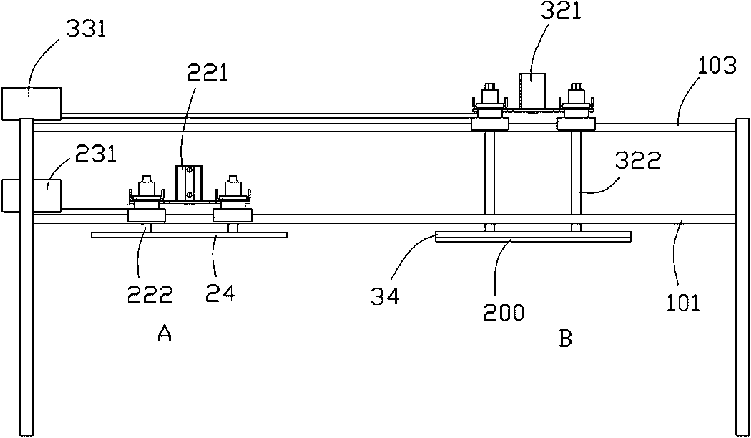
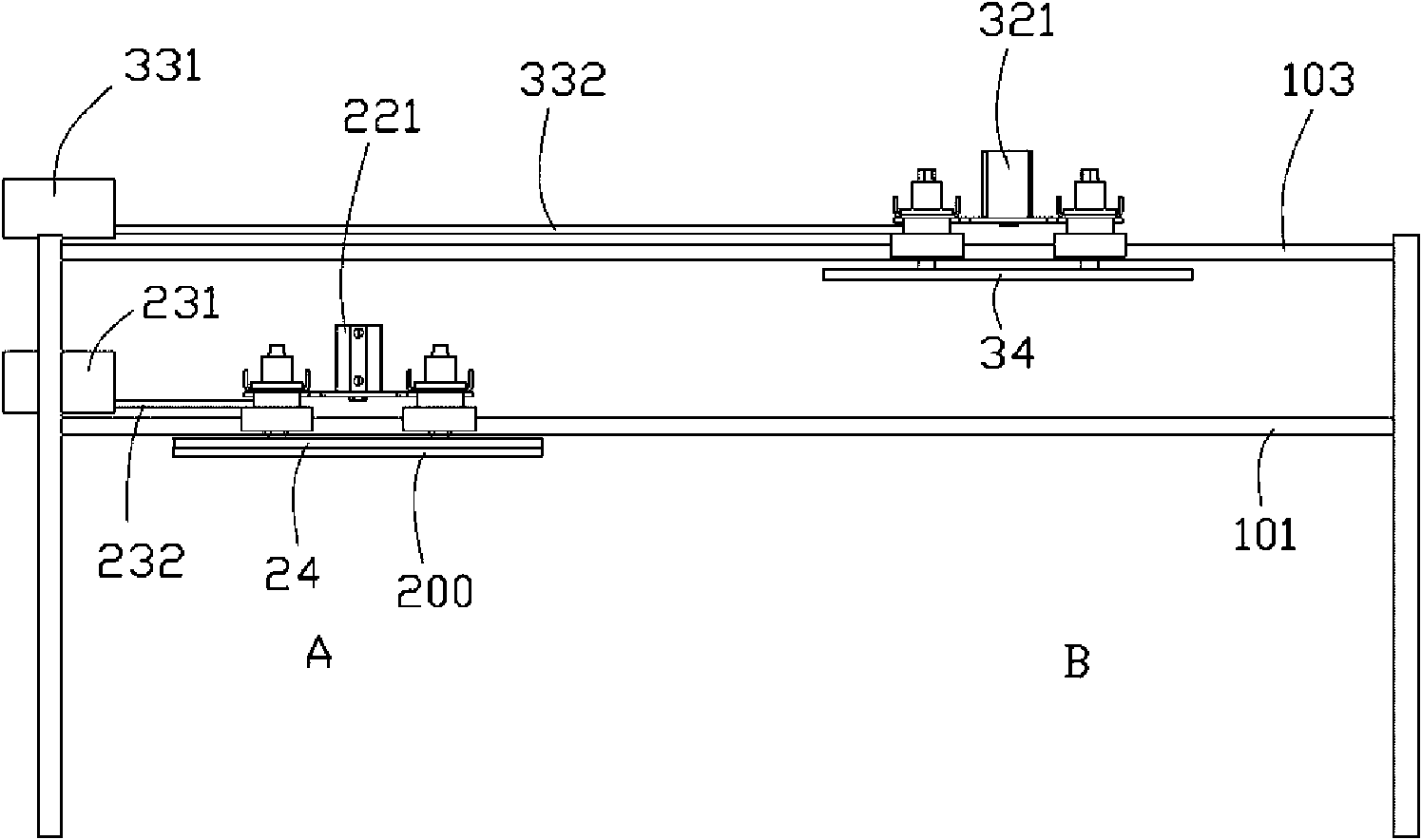
[0013] see figure 1 and figure 2 The embodiment of the technical solution provides a substrate transfer system 100, which includes a frame 10, a first driving device 22, a second driving device 23, a third driving device 32, a fourth driving device 33, a first adsorption device 24, The second adsorption device 34 , the first slider 21 and the second slider 31 .

[0014] The rack 10 includes a first guide rail 101 , a second guide rail 102 , a third guide rail 103 , a fourth guide rail 104 , four support rods 105 , a first connecting rod 106 and a second connecting rod 107 .

[0015] The first guide rail 101, the second guide rail 102, the third guide rail 103 and the fourth guide rail 104 are horizontally arranged and parallel to each other, wherein the first guide rail 101 and the second guide rail 102 are located in ...


PUM


Abstract

The invention relates to a substrate transfer system used for transferring a substrate positioned at a loading position to an unloading position. The substrate transfer system comprises a first adsorption device, a second adsorption device, a first driving device, a second driving device, a third driving device, a fourth driving device and a controller; and the controller controls the first adsorption device, the second adsorption device, the first driving device, the second driving device, the third driving device and the fourth driving device, so that the first adsorption device and the second adsorption device alternately adsorb the substrate positioned at the loading position, alternately transfer the substrate to the unloading position and lay down the substrate. The invention also relates to a substrate transfer method.

Description

technical field [0001] The invention relates to the field of flexible circuit board production, in particular to a substrate transfer system and method used in the production process of flexible circuit boards. Background technique [0002] With the miniaturization and high-speed performance of electronic products, circuit boards have developed from single-sided boards to double-sided boards and multi-layer boards. Among them, double-sided circuit boards and multilayer circuit boards have more wiring area and higher assembly density and are widely used. See literature: Takahashi, A.; High density multilayer printed circuit board for HITACM 880; IEEE Trans.on Components, Packaging, and Manufacturing Technology; 1992. [0003] The production of multi-layer circuit boards includes inner layer circuit making, inner layer inspection, lamination, drilling, electroplating, making conductive lines, line electroplating, outer layer inspection, solder mask, surface processing and cut...

Claims


Application Information

Patent Timeline
Patent Type & Authority Applications(China)
IPC IPC(8): H05K13/02H05K3/00
Inventor 沈家弘廖新治廖道明陈文村林承贤
Owner AVARY HLDG (SHENZHEN) CO LTD
Why Eureka
Try Eureka