Manufacturing method for protecting interval wall of bipolar transistor circuit

A technology of bipolar transistor and manufacturing method, applied in semiconductor/solid-state device manufacturing, circuits, electrical components, etc., can solve the problems of junction leakage current, low current gain β, prolonged dry etching time, etc.

Inactive Publication Date: 2014-09-24
RICHTEK TECH
View PDF3 Cites 0 Cited by
  • Summary
  • Abstract
  • Description
  • Claims
  • Application Information

AI Technical Summary

Problems solved by technology

It is known that the spacer process will prolong the dry etching time to ensure that the gate circuit 10 and the spacer material on the surface 18 of the silicon substrate can be etched clean, but the selectivity ratio of dry etching to TEOS 12 and silicon substrate 14 is very poor , tends to damage the silicon substrate surface 18 while etching the TEOS 12
[0004] image 3 It is a schematic diagram of the damage caused by the known spacer process to the BJT. When the damage to the silicon substrate surface caused by the aforementioned spacer process occurs at the p-n junction of the BJT 28, for example, at the emitter 24 and the base 22 of the BJT 28, or the collector When a defect 25 is formed between 20 and base 22, junction leakage current will be caused at these junctions
Since the base current provided to the BJT is generally only a few μA, and the junction leakage current caused by surface defects can usually reach the level of μA, the current gain β of the BJT 28 becomes very low
[0005] Therefore, there are above-mentioned inconveniences and problems in the known spacer process.

Method used


Image

  • Manufacturing method for protecting interval wall of bipolar transistor circuit
  • Manufacturing method for protecting interval wall of bipolar transistor circuit
  • Manufacturing method for protecting interval wall of bipolar transistor circuit

Examples


Embodiment Construction

[0026] The present invention will be further described below in conjunction with embodiment and accompanying drawing.

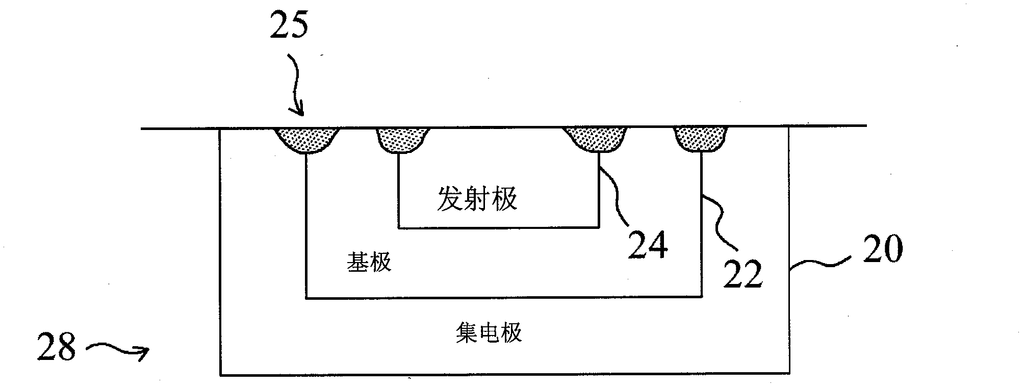
[0027] see now Figure 4 ~ Figure 7 , Figure 4 It is a structural schematic diagram of an embodiment of the present invention, Figure 5 is another structural schematic diagram of an embodiment of the present invention, Image 6 It is another structural schematic diagram of an embodiment of the present invention, Figure 7 It is another structural schematic diagram of the embodiment of the present invention. As shown in the figure, the silicon substrate 30 has a collector 38 and a base 36 of a BJT, and a gate 34 of a MOS transistor. After the spacer material layer 32 is deposited on the surface of the silicon substrate 30, an electrical The slurry or charged particles perform isotropic dry etching on the spacer material layer 32 . Such as Figure 5 As shown, when the spacer material layer 32 is dry-etched until the thin layer 40 is left, the dry etchin...


PUM


Abstract

The invention relates to a manufacturing method for protecting the interval wall of a bipolar transistor circuit. The bipolar transistor circuit and the grid circuit of an MOS transistor are arranged on the same substrate, and is characterized by comprising the following steps: the first step: depositing a layer of interval-wall material on the substrate; the second step: etching the interval-wall material layer dryly until a thin layer with preset thickness is left; and the third step: etching the thin layer wetly until the bipolar transistor circuit is exposed out. The manufacturing method for protecting the interval wall of the bipolar transistor circuit has the advantages of considering the integrity of the surface of the silicon substrate when removing excessive interval-wall material, improving junction leakage current and increasing the current gain beta of BJT.

Description

technical field [0001] The invention relates to a method for manufacturing an integrated circuit (IC), in particular to a method for manufacturing a spacer for protecting a bipolar transistor circuit. Background technique [0002] In current complementary metal oxide semiconductor (CMOS) manufacturing technology, spacer process (spacer process) is a common means to solve the hot carrier effect on MOS transistors. Transistors (BJTs) cause severe junction leakage. [0003] A typical spacer process is first to fully deposit a spacer material layer 12 on a silicon substrate 14 with a gate electrode 10, such as tetraethoxysilane (Tetra-Ethyl-Ortho-Silicate; TEOS), such as figure 1 as shown, figure 1 It is a schematic diagram of a known spacer process; then the spacer material layer 12 is etched by a dry etching process; figure 2 the spacer wall 16, figure 2 It is another schematic diagram of a known spacer process. It is known that the spacer process will prolong the dry e...

Claims


Application Information

Patent Timeline
Patent Type & Authority Patents(China)
IPC IPC(8): H01L21/8249H01L21/311
Inventor 詹前陵刘景萌苏宏德
Owner RICHTEK TECH
Why Eureka
Try Eureka