PCB design method and system automatically leading in design rule

A design method and rule technology, applied in the computer field, can solve the problems of low PCB design efficiency, difficulty in ensuring data accuracy, and inability to guarantee data, and achieve the effect of reducing repetitive labor, ensuring performance, and simplifying upgrades and maintenance.

Inactive Publication Date: 2010-02-24
SHANGHAI WINGTECH ELECTRONICS TECH
View PDF1 Cites 7 Cited by
  • Summary
  • Abstract
  • Description
  • Claims
  • Application Information

AI Technical Summary

Problems solved by technology

Therefore, the process of inputting design rules not only takes a lot of time, but also needs to comprehensively consider the enterprise specifications and the information conveyed by the production technologist, making it difficult to guarantee the accuracy of the data, and of course the data corresponding to the imported design rules cannot be guaranteed is the current optimal value
[0006] At the same time, for the PCB design rules input by CAD engineers, QA (Quality Assurance) engineers need to spend a lot of time checking the CAD engineer's design item by item, which further reduces the efficiency of PCB design.

Method used


Image

  • PCB design method and system automatically leading in design rule
  • PCB design method and system automatically leading in design rule
  • PCB design method and system automatically leading in design rule

Examples


Embodiment Construction

[0034] The preferred embodiments of the present invention are given below in conjunction with the accompanying drawings to describe the technical solution of the present invention in detail.

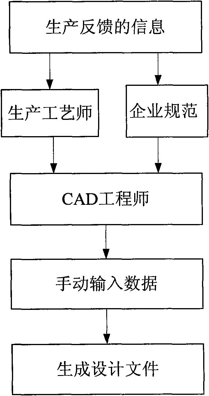
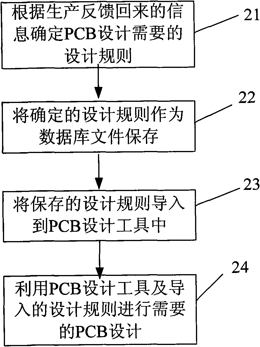
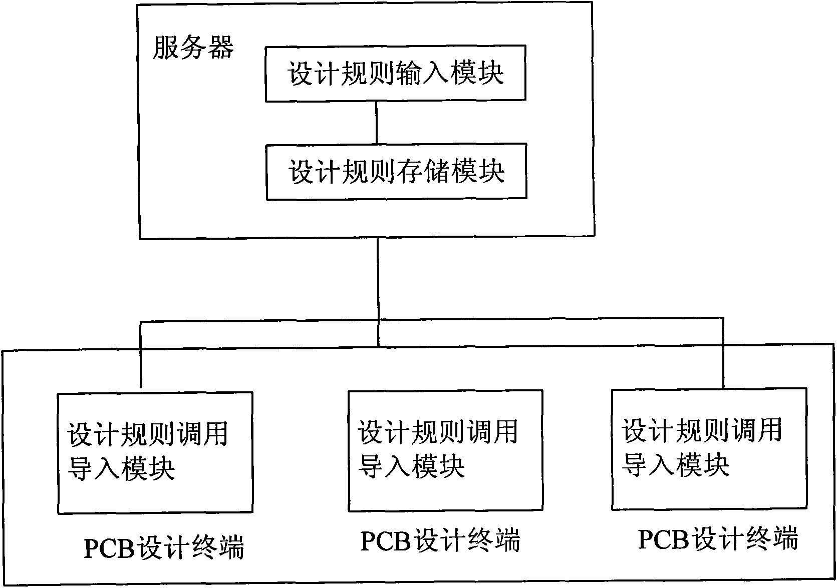
[0035] The core of the present invention is to save the design rules required by PCB design as a database file in a server that can be accessed by each PCB design terminal, such as the company's server. Save the design rules and import them into the corresponding PCB design files, so that the corresponding PCB design can be carried out based on the design rules. The design rules saved in the server are usually passed by the production technologist, CAD engineer expert, QA and ICT (Information and Communications Technology, information and communication technology) engineers and other analysis and evaluation, so the accuracy of the design rules can be well guaranteed, and the determined design rules can also be guaranteed to be the optimal value. In the present invention, after the design...


PUM


Abstract

The invention discloses a PCB design method and a system automatically leading in a design rule. The method comprises the following steps: S1. determining a design rule needed by PCB design and storing; S2. leading the stored design rule into a PCB design tool; S3. using the PCB design tool and the led-in design rule to perform necessary PCB design. The invention causes the design rule in the PCBdesign process to be conveniently led in and ensures the accuracy of the led-in design rule, so that PCB design is more standard, and the PCB design performance is ensured. Meanwhile, the invention also reduces the workload of CAD engineers, QA engineers and production technologists and is convenient to upgrade and maintain each PCB design rule.

Description

technical field [0001] The invention relates to the field of computer technology, in particular to a PCB (PCB Printed Circuit, printed circuit board) design method and system for automatically importing design rules. Background technique [0002] During the PCB design process, it is usually necessary to follow the corresponding design rules, such as the allowable spacing between device connections, the allowable width of the connection lines, etc. The design rules are usually recorded in the enterprise specifications, and the PCB design process is based on Enterprise norms are carried out. At present, the process of introducing the design rules adopted is as follows: figure 1 As shown, it includes: the production technologist formulates the enterprise specification for PCB design according to the feedback information in the PCB production process, and the PCB designer, that is, the CAD (computer-aided design) engineer introduces the design rules according to the enterprise ...

Claims


Application Information

Patent Timeline
Patent Type & Authority Applications(China)
IPC IPC(8): G06F17/50
Inventor 洪韶峰陈贤能
Owner SHANGHAI WINGTECH ELECTRONICS TECH
Why Eureka
Try Eureka