Transmission hole of matched high frequency broadband impedance

A technology of impedance matching and transmission holes, which is applied in the field of transmission holes, can solve the problems of reducing the flexibility of circuit applications and the difficulty of controlling the precision of the overall multi-layer printed circuit board.

Inactive Publication Date: 2010-03-03
IND TECH RES INST
View PDF0 Cites 24 Cited by
  • Summary
  • Abstract
  • Description
  • Claims
  • Application Information

AI Technical Summary

Problems solved by technology

However, this method will cause a lot of design complexity, reduce the flexibility of circuit applications, and the precision control of the overall multi-layer printed circuit board is not easy

Method used


Image

  • Transmission hole of matched high frequency broadband impedance
  • Transmission hole of matched high frequency broadband impedance
  • Transmission hole of matched high frequency broadband impedance

Examples


Embodiment Construction

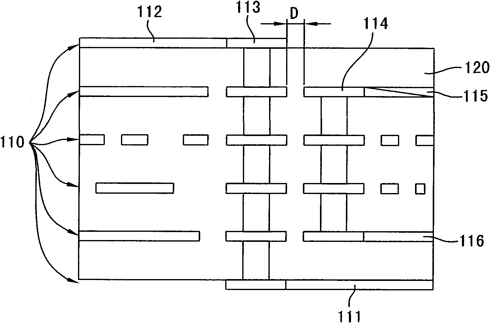
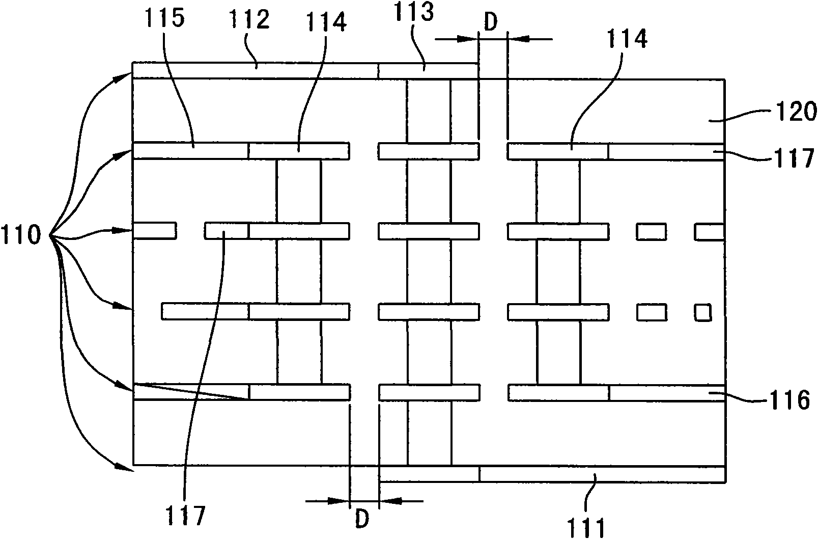
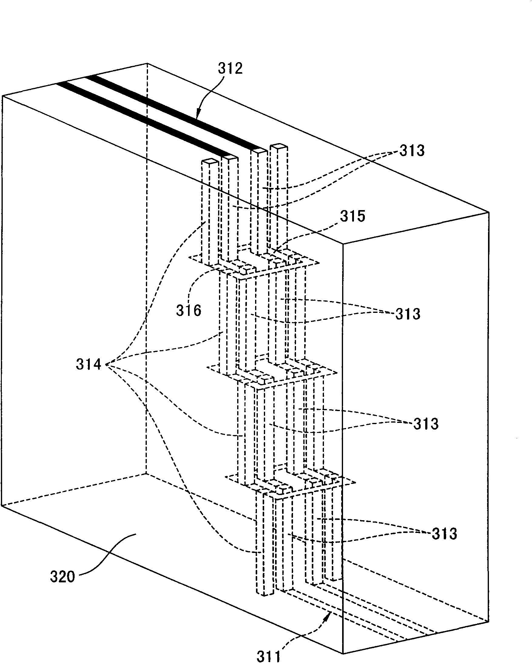
[0046] The high-frequency broadband impedance matching transmission hole disclosed by the present invention is applied to various substrates, such as multi-layer circuit boards, LTCC, IC, thick-film ceramics, thin-film ceramics, silicon substrate glass substrate manufacturing processes, etc., through the grounding via hole It is arranged around the signal via hole, so that the signal transmission of the vertical signal via hole has impedance matching. The following structure takes a multilayer circuit board as an example, and the multilayer circuit board achieves the purpose of impedance matching through structural design. The multi-layer circuit board structure is a combination of stacking multiple insulating layers and circuit layers, using vertical signal via holes to provide electrical connections to the circuit layers, and adding vertical ground via holes to the structure, so that the vertical signal via holes The signal transmission achieves impedance matching, and the e...


PUM


Abstract

The invention relates to a transmission hole of matched high frequency broadband impedance which takes a multi-layer printed circuit board as an example, is the combination of a plurality of circuit layers and insulating layers which are arranged in an interlacing and laminating way, comprises a plurality of signal transmission lines, vertical signal via holes and vertical grounding via holes, wherein all signal transmission lines are arranged in different circuit layers and connected with each other between the signal transmission lines by the vertical signal transmission holes and causes thevertical signal transmission holes to reach impedance matching by arranging the corresponding vertical grounding via holes.

Description

technical field [0001] The invention relates to a transmission hole, which is applied to multilayer circuit boards, LTCC, IC, thick-film ceramics, thin-film ceramics, silicon substrate glass substrate manufacturing processes, etc., and particularly relates to a transmission hole for high-frequency broadband impedance matching. Background technique [0002] In electronic system products, including circuit boards, low-temperature cofired ceramics (Low-TemperatureCofired Ceramics, LTCC), IC, thick film ceramics, thin film ceramics, silicon substrates and glass substrate processes, among which printed circuit boards (Printed Circuit Board, PCB), usually use a flat substrate composed of glass fiber cloth or soft substrate, and then print a conductive circuit. As electronic products move towards the design concept of "thin, thin and small", printed circuit boards are also developing towards small aperture, high density, multi-layer count, and thin lines. Among them, the multilaye...

Claims


Application Information

Patent Timeline
IPC IPC(8): H05K1/02H05K1/11H05K3/42H05K3/46
Inventor 卓威明翁卿亮赖颖俊陈昌升
Owner IND TECH RES INST
Why Eureka
Try Eureka