

Display and electronic apparatus
A display device and display circuit technology, which is applied to identification devices, static indicators, electrical digital data processing, etc., can solve the problems of difficulty in reducing size and high cost, and achieve S/N improvement, impact reduction, and noise reduction. Effect
- Summary
- Abstract
- Description
- Claims
- Application Information
AI Technical Summary
Problems solved by technology
Method used
Image

Examples
no. 1 example
[0127] Figure 4 is a simplified sectional view of the light receiving unit portion according to the first embodiment of the present invention.
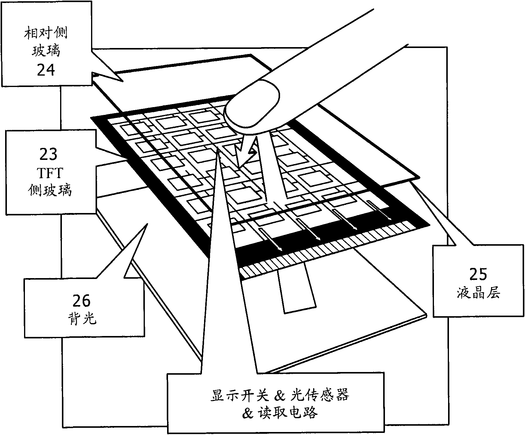
[0128] like Figure 4 As shown, the light receiving unit 22 is formed on the substrate surface 231 side of the TFT substrate 23 formed by using a transparent insulating substrate (for example, a glass substrate). As described above, the light receiving unit 22 includes the reading circuit and the light receiving element (photosensor) 221 .
[0129] The liquid crystal layer 25 is enclosed between the TFT substrate 23 and the opposite substrate 24 formed by using a relatively transparent insulating substrate (for example, a glass substrate). In addition, for example, a backlight 26 is placed on the bottom surface 232 side of the TFT substrate 23 .
[0130] In addition, a first polarizing plate 27 on the back side (lower side) is formed on the bottom surface 232 of the TFT substrate 23, and a second polarizing plate 28 on the front s...
no. 2 example
[0157] Figure 10 is a simplified sectional view of a light receiving unit portion according to a second embodiment of the present invention.
[0158] Figure 11 is a graph showing the spectrum of backlight light used in the second embodiment.
[0159] Figure 12 is a graph showing the spectral refractive index obtained by the antireflection treatment in the second embodiment.
[0160] Figure 13A and Figure 13B The structure and manufacturing process of the antireflection layer according to the second embodiment are shown.
[0161] In the second embodiment, as Figure 11 As shown, the backlight 26A emits light in the visible region and the infrared region, and as Figure 12 As shown, the anti-reflection layer 29A has been or has been subjected to an anti-reflection treatment optimized for light in the range from the visible region to the infrared region. Here, the infrared region means a region with a wavelength of not less than 700 nm.
[0162] like Figure 13B As...
no. 3 example
[0171] Figure 15 is a simplified sectional view of a light receiving unit portion according to a third embodiment of the present invention.
[0172] Figure 16 is a graph showing the spectral reflectance obtained by the antireflection treatment in the third embodiment.
[0173] Figure 17A ~ Figure 17D The structure and manufacturing process of the antireflection layer according to the third embodiment are shown.
[0174] In the third embodiment, a transparent protective cover (front-side transparent substrate) 31 is placed on the front side of the polarizing plate 28 with a filling layer 30 therebetween, and an anti-reflection layer 32 is placed between the front side of the protective cover 31 and the air layer at the interface.
[0175] In the third embodiment, such as Image 6 As shown, the backlight emits light in the visible region, and as Figure 16 As shown, the anti-reflection layer 32 has been or has been subjected to an anti-reflection treatment optimized for...
PUM
 Abstract
Description
Claims
Application Information