CMOS radio frequency (RF) switch based on silicon-on-insulator (SOI) technology

A silicon-on-insulator and RF switch technology, applied in transmission systems, electrical components, etc., can solve the problems of deteriorating the harmonic distortion index of RF switches, the inability to reduce the insertion loss of RF switches, and the impact of poor isolation performance, so as to suppress nonlinearity effect, good insertion loss and isolation performance, and the effect of shielding substrate noise

Inactive Publication Date: 2012-10-03
EAST CHINA NORMAL UNIV
View PDF0 Cites 2 Cited by
  • Summary
  • Abstract
  • Description
  • Claims
  • Application Information

AI Technical Summary

Problems solved by technology

[0006] Due to the limitation of process technology, the traditional bulk silicon CMOS RF switch cannot realize high-resistance substrate, reduce parasitic capacitance, and well control substrate noise
The insertion loss of the switch is directly related to the on-resistance and parasitic capacitance of the device, so the insertion loss of the RF switch cannot be greatly reduced on the traditional bulk silicon process
The isolation is closely related to the parasitic capacitance at both ends of the device. The high parasitic capacitance of the traditional bulk silicon process and the substrate that is easy to feed through will have a bad impact on the isolation performance
Multiple harmonics also appear in the form of substrate noise, deteriorating the harmonic distortion index of RF switches

Method used


Image

  • CMOS radio frequency (RF) switch based on silicon-on-insulator (SOI) technology
  • CMOS radio frequency (RF) switch based on silicon-on-insulator (SOI) technology
  • CMOS radio frequency (RF) switch based on silicon-on-insulator (SOI) technology

Examples


Embodiment Construction

[0026] The technical solution of the present invention is a specific embodiment, and the embodiment will not be repeated here. Describe the working process of the present invention in detail below.

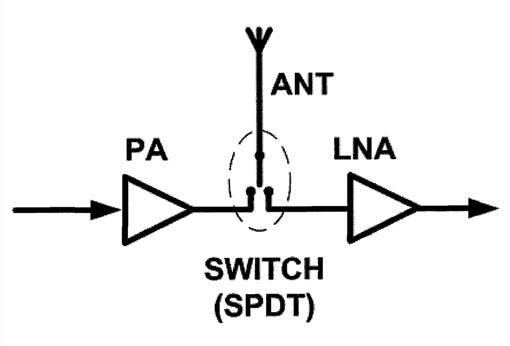
[0027] refer to Figure 4 , when the CT1 terminal is at a high level and the CT2 terminal is at a low level, the radio frequency switch of the present invention is in a transmitting mode. Since the gate voltages of the first MOS transistor M1 and the fifth MOS transistor M5 are positive, and the gate voltages of the third MOS transistor M3 and the seventh MOS transistor M7 are negative, the first MOS transistor M1 and the fifth MOS transistor M5 conduct pass, the third MOS transistor M3 and the seventh MOS transistor M7 are cut off, and the output signal of the power amplifier from the PA terminal can be transmitted to the antenna ANT terminal; since the gate voltage of the second MOS transistor M2 and the sixth MOS transistor M6 is negative, The gate voltages of the fourth MOS ...


PUM


Abstract

The invention discloses a CMOS radio frequency (RF) switch based on silicon-on-insulator (SOI) technology, which has the circuit structure adopting two-stage type closing isolation structure and two-stage type current release path structure, and utilizes a high resistance substrate and a buried oxide layer of an SOI technical device, thus remarkably reducing crosstalk and minimized parasitic capacitance, better screening substrate noise, obtaining ideal insertion loss and insulation performance at the two ends of the switch, inhibiting nonlinear effect and reducing harmonic distortion. The RFswitch has the circuit structure, reduces the channel resistance of a transistor connected in series, reduces the insertion loss, and further improves the closing performance of a transmitting terminal and a receiving terminal; furthermore, the switch can improve the insulation, leads harmonic quantity of every time to be in good grounding, improves the harmonic current of the substrate and inhibits harmonic component.

Description

technical field [0001] The invention relates to the technical field of integrated circuit design and signal processing, in particular to a complementary metal oxide semiconductor (CMOS) radio frequency switch based on silicon-on-insulator technology. Background technique [0002] With the rapid development of wireless communication technology, the current main process technologies in radio-frequency (Radio-Frequency, RF) applications include gallium arsenide (GaAs), silicon germanium (SiGe) BiCMOS and traditional bulk silicon CMOS technology, GaAs technology is expensive Due to the limited application cost of the market, SiGe BiCMOS technology and traditional bulk silicon CMOS technology are the mainstream of the market, and the traditional bulk silicon CMOS technology is favored for its low cost, low power consumption and easy process compatibility. However, the limitations of traditional bulk silicon CMOS technology in terms of noise and characteristic frequency make it no...

Claims


Application Information

Patent Timeline
Patent Type & Authority Patents(China)
IPC IPC(8): H04B1/44
Inventor 陈磊周进赖宗声马和良田亮黄爱波王超顾彬阮颖崔建明
Owner EAST CHINA NORMAL UNIV
Why Eureka
Try Eureka