Semiconductor device and method of manufacturing the same

A technology for semiconductors and devices, which is applied in the field of manufacturing semiconductor devices, can solve the problems of increased man-hours, etc., and achieve the effects of suppressing changes in coating thickness and suppressing the deterioration of adhesion

Inactive Publication Date: 2010-05-26
RENESAS ELECTRONICS CORP
View PDF1 Cites 7 Cited by
  • Summary
  • Abstract
  • Description
  • Claims
  • Application Information

AI Technical Summary

Problems solved by technology

Each of the methods described in Japanese Laid-Open Patent Publication No. 2006-080234, No. 2005-150690, and No. 2005-317804 requires an additional metal film to be formed between the barrier metal film and the interconnection, thereby requiring increased man-hours

Method used


Image

  • Semiconductor device and method of manufacturing the same
  • Semiconductor device and method of manufacturing the same
  • Semiconductor device and method of manufacturing the same

Examples


Embodiment Construction

[0019] Now, the present invention will be described herein with reference to exemplary embodiments. Those skilled in the art will recognize that many alternative embodiments can be accomplished using the teachings of the present invention and that the invention is not limited to the embodiments illustrated for explanatory purposed.

[0020] Embodiments of the present invention will be described below with reference to the accompanying drawings. Note that any similar components in all drawings will be denoted by like reference numerals or symbols, and descriptions thereof will not be repeated.

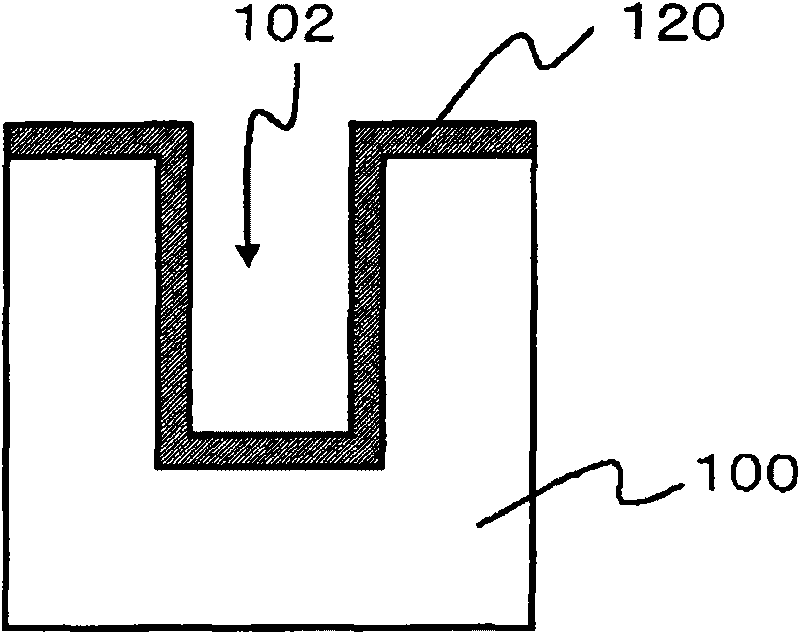
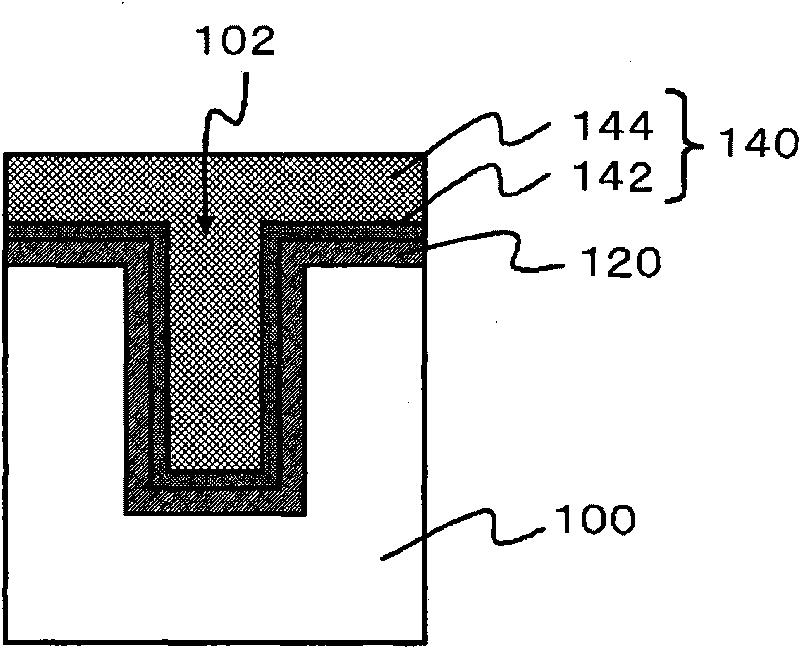
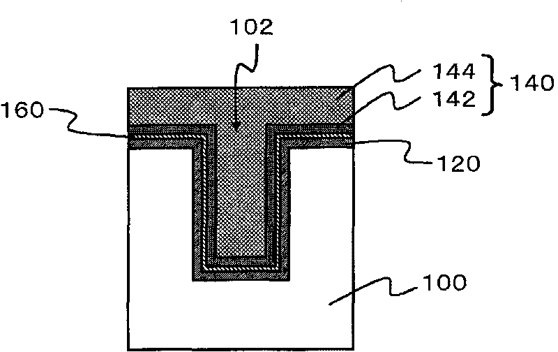
[0021] Figure 1A , Figure 1B , Figure 2A and Figure 2B is a cross-sectional view illustrating a method of manufacturing a semiconductor device according to the first embodiment. The method of manufacturing a semiconductor device has the steps described below. First, trench 102 is formed in insulating film 100 formed over a semiconductor substrate (not shown). Next, a barrier ...


PUM

PropertyMeasurementUnit
thicknessaaaaaaaaaa

Abstract

The invention provides a semiconductor device and method of manufacturing the same. A metal barrier film which contains an additive element is formed on the side face and on the bottom of a trench formed in an insulating film; a seed film is formed over the metal barrier film; a plated layer (Cu film) is formed using the seed film as a seed so as to fill up the trench with a metal film; the metal barrier film and the metal film are annealed to thereby form therebetween an alloy layer which contains a metal composing the metal barrier film, the additive element, and a metal composing the metal film, and to thereby allow the additive element to diffuse into the metal film.

Description

[0001] Cross References to Related Applications [0002] This application is based on Japanese Patent Application No. 2008-252455, the contents of which are hereby incorporated by reference. technical field [0003] The present invention relates to a semiconductor device having interconnections buried in an insulating film, and a method of manufacturing the semiconductor device. Background technique [0004] It is known that an interconnection structure of a semiconductor device is configured to fill a trench formed in an insulating film with a conductive layer (for example, a Cu layer). In the interconnection thus constructed, a barrier film (diffusion barrier film) is provided between the interconnection and the insulating film for the purpose of blocking the diffusion of the metal constituting the conductive layer into the insulating film. The provision of the barrier film presents a need to ensure adhesion between the interconnection and the barrier film. On the other ...

Claims


Application Information

Patent Timeline
Patent Type & Authority Applications(China)
IPC IPC(8): H01L21/768H01L23/532
CPCH01L23/53295H01L21/76843H01L21/76883H01L21/76873H01L21/76846H01L21/76858H01L23/53238H01L2924/0002H01L2924/00H01L21/3205H01L21/768
Inventor 黑川哲也户原诚人
Owner RENESAS ELECTRONICS CORP
Why Eureka
Try Eureka