Manufacturing method of monolithic integrated pressure sensor

A technology of pressure sensor and monolithic integration, which is applied in semiconductor/solid-state device manufacturing, measurement of the property and force of applied piezoresistive materials, electrical components, etc., and can solve compatibility difficulties, monolithic integration difficulties, and easy-to-contaminate IC processes, etc. problem, to achieve the effect of solving the compatibility of processing technology

Inactive Publication Date: 2010-06-02
NO 24 RES INST OF CETC
View PDF0 Cites 6 Cited by
  • Summary
  • Abstract
  • Description
  • Claims
  • Application Information

AI Technical Summary

Problems solved by technology

[0007] However, the piezoelectric thin-film resistive pressure sensor made by thin-film piezoresistive technology is difficult to realize monolithic integration with the amplification processing circuit. The main reason is that when the piezoelectric thin-film material deposition and corrosion processing are compatible with IC processing, it is easy to contaminate the IC. process, causing IC leakage
The capacitive pressure sensor made by capacitive technology is difficult to be compatible with IC processing technology due to deep groove corrosion, silicon glass bonding and other bulk silicon technologies, so it is also difficult to achieve monolithic integration with the amplification processing circuit
However, the resistive pressure sensor produced by silicon resistive technology and the amplification processing circuit are monolithically integrated, and there is also the difficulty of how to organically combine the processing technology of the pressure sensor with the processing technology of the amplification circuit. In the actual process, it is difficult Do not affect each other, therefore, it is also difficult to achieve monolithic integration

Method used


Image

  • Manufacturing method of monolithic integrated pressure sensor
  • Manufacturing method of monolithic integrated pressure sensor
  • Manufacturing method of monolithic integrated pressure sensor

Examples


Embodiment Construction

[0064] Specific embodiments of the present invention are not limited to the following description. The present invention will be further described now in conjunction with accompanying drawing.

[0065] The main steps of the inventive method are as follows:

[0066] 1. On the P-type silicon substrate sheet 2, the steps of making the P-type silicon substrate that bipolar analog integrated circuits and varistors are used are as follows:

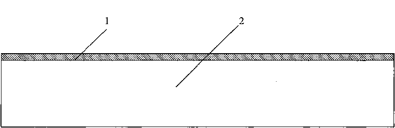
[0067] (1) P-type silicon substrate 2, with crystal orientation, polished on both sides, with a thickness of 400±10 μm and a resistivity of 7-13Ω·cm, cleaned and oxidized, and the thickness of the oxide layer 1 is 0.6±0.05 μm, such as figure 1 shown;

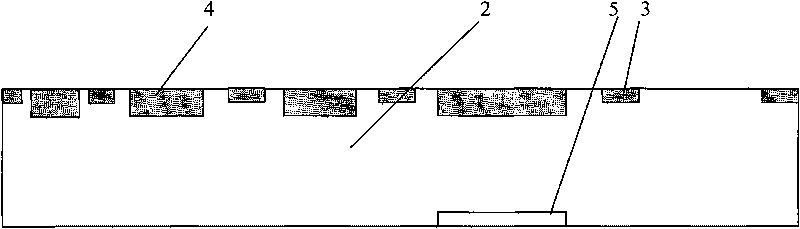
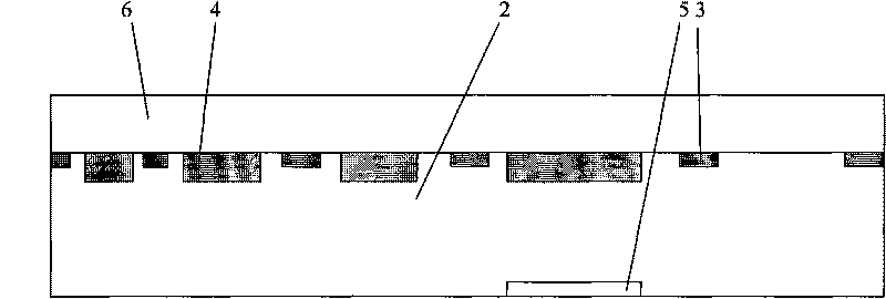
[0068] (2) photoetching N+ buried layer region 3;

[0069] (3) Adhesive arsenic injection, dose 6E15 / cm 2 , energy 100keV, glue removal;

[0070] (4) photoetching P+buried layer region 4;

[0071] (5) Boron injection with glue, dose 1E15 / cm 2 , energy 60keV, glue removal;

[0072] (6) Usi...


PUM

PropertyMeasurementUnit
Resistivityaaaaaaaaaa

Abstract

The invention discloses a manufacturing method of a monolithic integrated pressure sensor. Te In the invention, overcomes the problem of processing technology compatibility of a resistance type pressure sensor and an amplification processing circuit is solved, combines the processing technology of the resistance type pressure sensor and the processing technology of the amplification processing circuit are combined, and utilizes a special clamp for protecting an integrated circuit and a piezoresistor on the front surface are utilized, meanwhile, a deep slot is formed below the piezoresistor through corrosion, so that the piezoresistor is successfully manufactured on a movable silicon film, . The invention solvessolving the technical difficult problem of processing technology compatibility of the pressure sensor and the circuit, and realizing realizes the monolithic integration of the pressure sensor and the circuit. The method is suitable for the processing field of miniaturized high-reliability pressure sensors.

Description

technical field [0001] The invention relates to a manufacturing method of a monolithic integrated pressure sensor. It is suitable for the processing field of miniaturized and highly reliable pressure sensors. Background technique [0002] At present, in the semiconductor pressure sensor manufacturing technology, the methods of manufacturing pressure sensors mainly include: [0003] 1. Thin film piezoresistive technology. It grows a layer of pressure-sensitive piezoelectric thin film material on a silicon wafer substrate, photoresistively etches piezoresistive regions, sputters metal leads, photoetches metal leads, and alloys to produce a thin film pressure sensor. It uses a pressure-sensitive piezoelectric film material to detect pressure, thereby forming a piezoelectric film resistive pressure sensor. [0004] 2. Silicon resistive technology. It produces P-type diffused resistors on N-type silicon wafers through oxidation, photolithography, P-type diffusion and other se...

Claims


Application Information

Patent Timeline
IPC IPC(8): H01L21/8222G01L1/18
Inventor 张正元梅勇冯志成李建根李小刚徐勇
Owner NO 24 RES INST OF CETC
Why Eureka
Try Eureka