Method for manufacturing monolithic polysilicon cantilever structure

A manufacturing method and polysilicon technology are applied in the field of monolithic manufacturing of polysilicon cantilever beam structures and monolithic integrated manufacturing of polysilicon cantilever beam structures and BiCMOS signal processing circuits, which can solve the problems of difficult process realization and high cost.

Inactive Publication Date: 2011-06-08
NO 24 RES INST OF CETC
View PDF5 Cites 13 Cited by
  • Summary
  • Abstract
  • Description
  • Claims
  • Application Information

AI Technical Summary

Problems solved by technology

For example, the high-temperature process steps involved in the manufacture of MEMS microstructures can be completed before the CMOS metallization process, that is, the MEMS high-temperature process is embedded into the standard CMOS process steps, so that the MEMS high-temperature process will not affect the CM

Method used


Image

  • Method for manufacturing monolithic polysilicon cantilever structure
  • Method for manufacturing monolithic polysilicon cantilever structure
  • Method for manufacturing monolithic polysilicon cantilever structure

Examples


Embodiment Construction

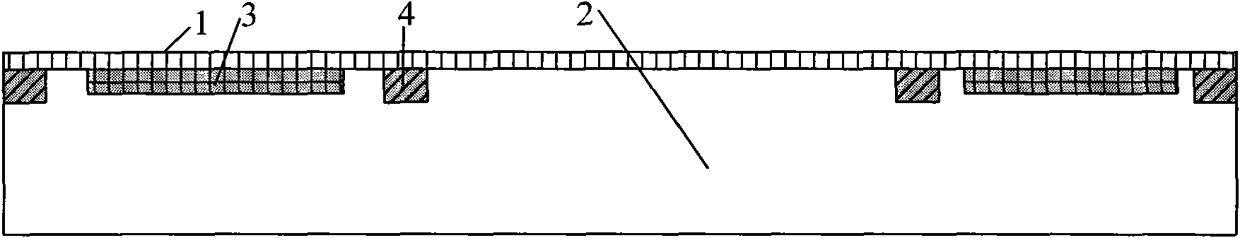
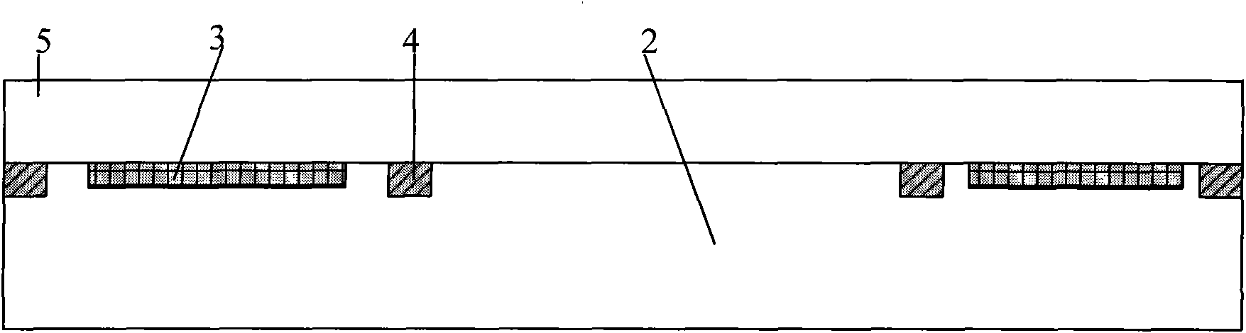
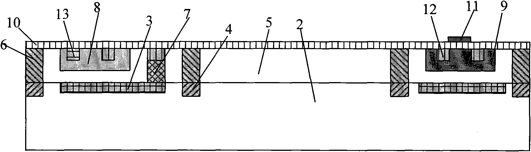
[0116] The specific embodiment of the present invention is not limited to the following description, the present invention is further described in conjunction with the accompanying drawings, wherein the detailed steps of a specific embodiment are as follows:

[0117] 1. On the P-type substrate sheet 2, the steps of making a conventional BiCMOS signal processing circuit are as follows:

[0118](1) Select a P-type silicon substrate 2 with a crystal orientation of , a thickness of 525±20 μm, and a resistivity of 7-13Ω·cm, clean and oxidize, and the thickness of the oxide layer is 0.6±0.05 μm;

[0119] (2) photoetching N+ buried layer region 3;

[0120] (3) Wet etching, removing the oxide layer above the N+ buried layer region 3, and removing the glue;

[0121] (4) cleaning, oxidation, the thickness of oxide layer is 14-18nm;

[0122] (5) photoetching the N+ buried layer region 3;

[0123] (6) Adhesive arsenic injection, dose 3.2E15 / cm 2 , energy 100keV, glue removal;

[0124...


PUM

PropertyMeasurementUnit
Thicknessaaaaaaaaaa
Thicknessaaaaaaaaaa
Thicknessaaaaaaaaaa

Abstract

The invention relates to a method for manufacturing a monolithic polysilicon cantilever structure. In the invention, a processing step of the polysilicon cantilever structure is inserted in a conventional BiCMOS (Bipolar Complementary Metal Oxide Semiconductor) technical process, the deposition and the annealing of polysilicon are finished and an MEMS (Micro-Electro-Mechanical Systems) high-temperature process is prevented from influencing on the metalation process before the metalation process. In the release process of the polysilicon cantilever structure, a special etching solution is adopted, and a negative photoresist is used as a post of the polysilicon cantilever structure so as to effectively avoid the problem of substrate adhesion in the cantilever structure release process by using a wet method. The method provided by the invention solves the technical problems of compatibility between a manufacture process of the polysilicon cantilever structure and a processing process of a BiCMOS circuit, realizes the monolithic integration of the polysilicon cantilever structure and a BiCMOS signal processing circuit, and can be widely applied to the monolithic integration manufacture field of MEMS sensors, such as capacitive accelerometers, gyroscopes, and the like.

Description

technical field [0001] The present invention relates to a monolithic manufacturing method of a polysilicon cantilever structure, in particular to a monolithic integrated manufacturing method of a polysilicon cantilever structure and a BiCMOS signal processing circuit, which is directly applied to monolithic MEMS sensors such as capacitive accelerometers and gyroscopes integrated manufacturing field. Background technique [0002] MEMS sensors usually include two parts, MEMS microstructure and signal processing circuit. There are generally two methods to realize the electrical connection between the two. One is the hybrid integration method, that is, MEMS microstructure and signal processing circuit are produced separately, and then The finished two chips are hybrid-integrated on a PCB or a ceramic substrate, and packaged into a housing. The biggest advantage of this method is that it avoids the problem of process compatibility and greatly reduces the difficulty of process de...

Claims


Application Information

Patent Timeline
IPC IPC(8): B81C1/00
Inventor 李小刚李健根梅勇张正元
Owner NO 24 RES INST OF CETC
Why Eureka
Try Eureka