Semiconductor grid drive circuit and drive method thereof

A technology of gate drive circuit and drive method, applied in instruments, static indicators, etc., can solve problems such as large production space and complex structure

Active Publication Date: 2012-05-30
HANNSTAR DISPLAY CORPORATION
View PDF1 Cites 0 Cited by
  • Summary
  • Abstract
  • Description
  • Claims
  • Application Information

AI Technical Summary

Problems solved by technology

However, since each driving stage of the shift register still includes six thin film transistors, it has a more complex structure and requires a larger manufacturing space

Method used


Image

  • Semiconductor grid drive circuit and drive method thereof
  • Semiconductor grid drive circuit and drive method thereof
  • Semiconductor grid drive circuit and drive method thereof

Examples


Embodiment Construction

[0043] In order to make the above and other objects, features, and advantages of the present invention more apparent, the following will be described in detail with reference to the embodiments shown in the accompanying drawings. In addition, in the descriptions of the various embodiments of the present invention, the same or similar components are represented by the same symbols.

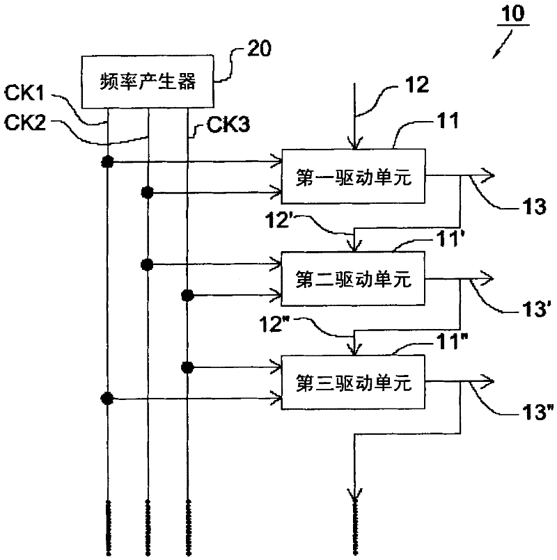
[0044] Please refer to Figure 2a , which shows a block diagram of a semiconductor gate driving circuit 10 according to an embodiment of the present invention. The semiconductor gate driving circuit 10 includes a plurality of driving units connected in series, such as the first driving unit 11 (as a first-level driving unit), the second driving unit 11 ′ and the third driving unit 11 ″ shown in the figure, etc., and receive an input signal and a plurality of frequency signals, wherein the frequency signal is provided by the frequency generator 20 , and the frequency generator 20 may or may not be in...


PUM


Abstract

The invention discloses a semiconductor grid drive circuit which receives a plurality of frequency signals and comprises a plurality of drive units which are connected in series, wherein each drive unit is used for driving a load and comprises an input end, an output end, a first switch and a second switch; the first switch is provided with a first end coupled with the input end, a second end coupled with a first node and a control end for receiving the first frequency signal and is switched on when the first frequency signal is in a high potential; the second switch is provided with a first end for receiving the second frequency signal, a second end coupled with the output end and a control end coupled with the first node; when the first node is in a high potential, the second frequency signal charges and discharges the load by the second switch; and the output end of each drive unit is coupled to the input end of the next stage drive unit.

Description

technical field [0001] The invention relates to a gate drive circuit, in particular to a semiconductor gate drive circuit for a liquid crystal display. Background technique [0002] The liquid crystal display 9 generally includes a pixel matrix 91, a plurality of gate drive circuits 92 and a plurality of source drive circuits 93, such as Figure 1a shown. The pixel matrix 91 includes a plurality of gate lines, a plurality of data lines and pixel units (not shown) located at the junctions of the gate lines and the data lines. Each gate driving circuit 92 is coupled to a column of pixel units through a gate line to sequentially provide scanning signals to the pixel matrix 91; the source driving circuit 93 is connected to a row of pixel units through a data line to provide the scanning signal to the Each pixel of the column that is turned on supplies the gray scale voltage to be displayed. [0003] In order to make the image quality displayed by the liquid crystal display cle...

Claims


Application Information

Patent Timeline
Patent Type & Authority Patents(China)
IPC IPC(8): G09G3/20G09G3/36
Inventor 陈彦州卢永信游家华林松君
Owner HANNSTAR DISPLAY CORPORATION
Why Eureka
Try Eureka