Copper indium gallium selenium (CIGS) solar cell, film of absorbing layer thereof, method and equipment for preparing film

A technology of solar cells and copper indium gallium selenide, applied in circuits, photovoltaic power generation, electrical components, etc., can solve the problems of uneven distribution of In and Ga elements, and achieve the effects of assembly line operation, cost reduction, and simple process

Inactive Publication Date: 2010-06-16
北京华仁合创科技有限公司
View PDF1 Cites 32 Cited by
  • Summary
  • Abstract
  • Description
  • Claims
  • Application Information

AI Technical Summary

Problems solved by technology

[0006] The technical problem to be solved by the present invention is to provide a method and equipment for preparing a copper indium gallium selenide (CIGS) absorber film for a copper indium gallium selenide solar cell and the copper indium gallium sele

Method used


Image

  • Copper indium gallium selenium (CIGS) solar cell, film of absorbing layer thereof, method and equipment for preparing film
  • Copper indium gallium selenium (CIGS) solar cell, film of absorbing layer thereof, method and equipment for preparing film
  • Copper indium gallium selenium (CIGS) solar cell, film of absorbing layer thereof, method and equipment for preparing film

Examples


example 1

[0043] Example 1: the present invention's process can be as attached Figure 5 implemented in the vacuum apparatus shown. The system consists of three vacuum chambers A, B, and C, and A and B, B and C are isolated by gate valves. The sample is fixed vertically on the sample holder, the side of the sample with the Mo film faces the positive direction of the vacuum chamber, the sample holder is driven by the rack, and can freely move in translation in the three vacuum chambers. In the vacuum chamber A, a Cu / Ga alloy target (Ga atomic content 20% to 40%) and a pure In target are set in the forward direction for sputtering and depositing metal films, and there is a resistance wire heater in the reverse direction, which can Heat the sample. There is a Se evaporation line source in the forward direction of the vacuum chamber B, and a heater in the reverse direction to provide a substrate temperature of 250-400°C, which can complete the evaporation of selenium and selenization. Ch...

example 2

[0044] Example 2: This example is the assembly line of the process of Example 1, and the system is composed of A 1 B 1 A 2 B 2 ......A n B n C, as attached Figure 6 , where A 1 、A 2 ~A n structure and attached Figure 5 The vacuum chambers A are identical to those of B 1 , B 2 ~B n with attached Figure 5 Vacuum chamber B is consistent. In this way, the sample can move in one direction in the system to realize the pipeline.

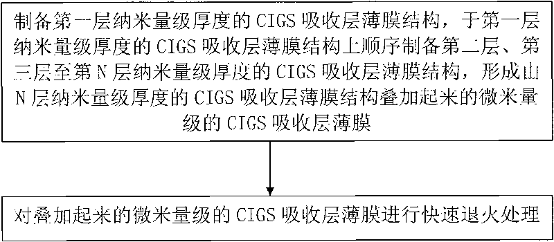
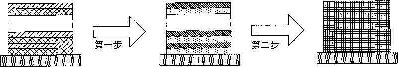
[0045] The effect of the preparation method of the present invention: the core technology of the present invention is to adopt partial selenization and then unified annealing. Compared with other techniques for preparing copper indium gallium selenide (CIGS) thin films, it mainly has the following advantages: first, micron-scale The copper indium gallium selenide (CIGS) absorbing layer film of the company is formed by stacking multiple nanoscale copper indium gallium selenide (CIGS) film structures, which can effectively prevent the uneven ...


PUM


Abstract

The invention provides a method for preparing a film of an absorbing layer of a copper indium gallium selenium (CIGS) solar cell, which comprises the following steps: 1, depositing a copper indium gallium (CIG) ternary metallic film, evaporating a selenium film to form a nanometer grade CIGS film structure, ensuring the temperature of a Se evaporating source is between 260 and 300 DEG C, and repeating the step for 10 to 50 times; and 2, carrying out quick annealing treatment on the superposed CIGS absorbing layer film to prepare the nanometer grade polycrystalline CIGS film. The method has the advantages that the proportion of various elements can be accurately controlled; compared with other methods for preparing the CIGS films, each element is distributed uniformly in the whole thickness range of the film with small change gradient; the whole technical process is simple and convenient, and is suitable for large-scale continuous production. Furthermore, the invention also discloses the CIGS absorbing layer film of the CIGS solar cell, the solar cell containing the CIGS absorbing layer film of the CIGS solar cell, and the manufacturing equipment used in the method.

Description

technical field [0001] The present invention relates to a preparation scheme for semiconductor materials used in solar cells, in particular to a method and equipment for preparing a copper indium gallium selenium solar cell absorber film, and the copper indium gallium selenide absorber film obtained by the method and the absorber layer containing the absorber Thin film solar cells. Background technique [0002] Copper indium gallium selenide (CIGS) solar cell is a multi-component compound semiconductor thin film cell. It is a photovoltaic device composed of sequentially depositing multiple layers of thin films on glass or other cheap substrates. Its structure is as attached figure 1 shown. From the glass substrate to the top layer in order: metal Mo back electrode / copper indium gallium selenide (CIGS) absorption layer / CdS transition layer / intrinsic ZnO (i-ZnO) layer / ZnO:Al window layer, and finally can be selected on the surface The anti-reflection layer (AR Coating) is pl...

Claims


Application Information

Patent Timeline
IPC IPC(8): H01L31/18H01L31/0216H01L31/032H01L31/042C03C17/36H01L31/0445H01L31/0749
CPCY02E10/50Y02E10/541Y02P70/50
Inventor 夏莹菲赵夔陆贞冀
Owner 北京华仁合创科技有限公司
Why Eureka
Try Eureka