Method for evaluating displacement damage of radiation of CMOS device

A displacement damage and device technology, applied in semiconductor/solid-state device manufacturing, instrumentation, computing, etc., can solve problems such as changes affecting threshold voltage, inaccurate methods, and inability to meet irradiation technology.

Inactive Publication Date: 2010-06-30
SEMICONDUCTOR MANUFACTURING INTERNATIONAL (BEIJING) CORP +1
View PDF0 Cites 7 Cited by
  • Summary
  • Abstract
  • Description
  • Claims
  • Application Information

AI Technical Summary

Problems solved by technology

Many circuits such as SRAM cells, sensitive amplifiers, and some digital and analog circuits require symmetry of device parameters, and the change of impurity concentration caused by irradiation will affect the change of threshold voltage and make the device parameters mismatch, thus seriously affecting the performance of the circuit.
[0004] Therefore, with the improvement of circuit integration, the method used to predict the single event effect of devices and integrated circuits is no longer accurate. Cannot meet the application of current irradiation technology

Method used


Image

  • Method for evaluating displacement damage of radiation of CMOS device
  • Method for evaluating displacement damage of radiation of CMOS device
  • Method for evaluating displacement damage of radiation of CMOS device

Examples


Embodiment Construction

[0020] The preferred embodiments of the present invention will be described in more detail below with reference to the accompanying drawings of the present invention.

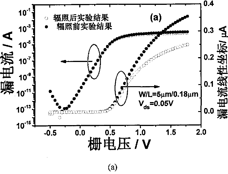
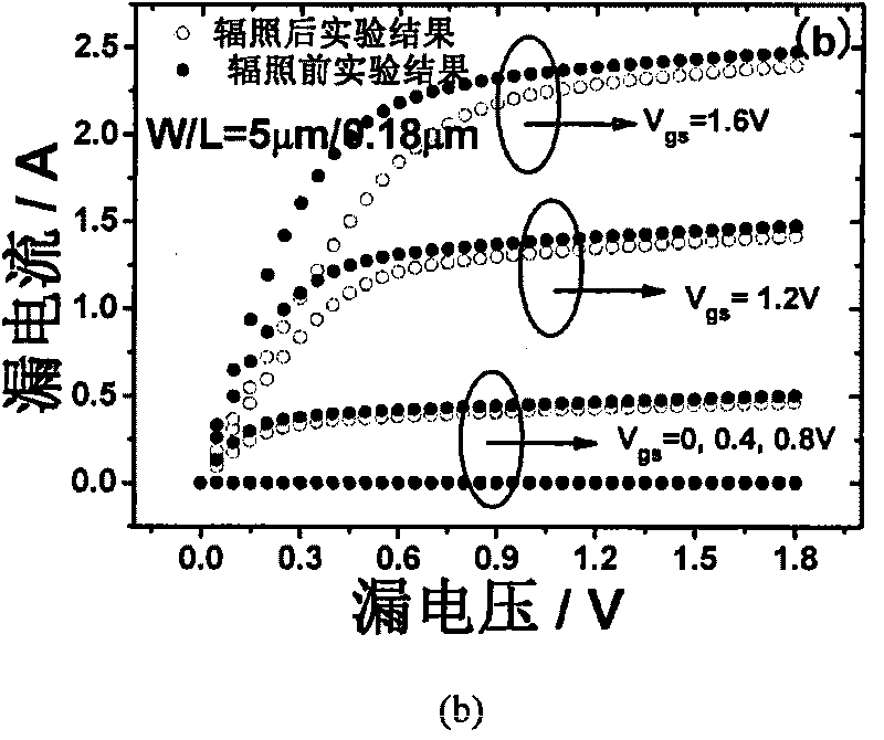
[0021] The present invention uses the Monte Carlo method to randomly generate incident particles according to Gaussian distribution, and establishes a calculation formula according to the incident particles hitting three different positions of the source and drain ends of the device, the channel region and the isolation region: I ds =prob1×case1+prob2×case2+prob3×case3, estimate the displacement damage of the CMOS device in the radiation environment. The specific estimation steps are as follows:

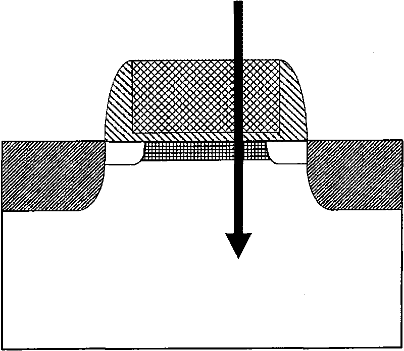
[0022] 1. When a single particle hits the source and drain terminals of the CMOS device, the parasitic resistance of the source and drain terminals increases. As the channel length of the MOS transistor decreases, the intrinsic resistance of the channel decreases, while the parasitic resistance of the source and drain regio...


PUM


Abstract

The present invention provides a method for evaluating displacement damage of radiation of CMOS devices, which belongs to the technical field of displacement damage of radiation of CMOS devices. The method is characterized in that a computing formula: Ids=prob1 x case1+prob2 x case2+prob3 x case3, is established according to three different positions on a device drain terminal, a channel region and an isolation region where incident particles hit, wherein the case indicates the current variation of the drain terminal of the device caused by the displacement damage generated when incident particles hit different positions on the device, and prob indicates the probability that the incident particle hit different positions on the device. According to the formula, the current variation Ids of the drain terminal of the device caused by the displacement damage can be worked out, and thus the displacement damage of a CMOS device in a radiation environment can be estimated. The displacement damage effect of devices and integrated circuits in a radiation environment can be estimated exactly by method.

Description

Technical field [0001] The invention relates to the radiation displacement damage of a CMOS device, in particular to a method for estimating the influence of the displacement damage effect on the electrical characteristics of the CMOS device. Background technique [0002] For decades, CMOS integrated circuits have been developing continuously following Moore's Law. By reducing the size of the device, the integration is continuously improved. As the feature size of the device shrinks, the device performance is constantly changing and developing. However, the reduction in device feature size also brings various small size effects and reliability issues. The small size effect mainly includes serious degradation of sub-threshold characteristics, DIBL (drain-induced barrier reduction), and the threshold voltage is related to the channel length to a very serious degree; reliability problems mainly include hot carrier effects, oxide layer degradation over time Breakdown (TDDB) and de...

Claims


Application Information

Patent Timeline
Patent Type & Authority Applications(China)
IPC IPC(8): G06F17/50H01L21/8238
Inventor 薛守斌王思浩黄如张兴
Owner SEMICONDUCTOR MANUFACTURING INTERNATIONAL (BEIJING) CORP
Why Eureka
Try Eureka