Method for detecting adhesive force of metal layer on back of wafer

A backside metal and detection method technology, applied in semiconductor/solid-state device testing/measurement, etc., can solve the problems of inability to quantitatively measure the adhesion of the metal layer on the backside of the wafer, high detection cost, and expensive blue film price, etc., to achieve accurate measurement results Reliable, simple detection method, low cost effect

Inactive Publication Date: 2010-08-25
SHANGHAI HUAHONG GRACE SEMICON MFG CORP
View PDF3 Cites 7 Cited by
  • Summary
  • Abstract
  • Description
  • Claims
  • Application Information

AI Technical Summary

Problems solved by technology

[0004] The method for detecting the adhesion of the metal layer on the back of the wafer in the prior art has the following disadvantages: first, this method can only qualitatively determine whether the adhesion of the metal layer on the back of the wafer meets the production requirements, and cannot quantitatively measure the adhesion of the metal layer on the back of the wafer. Moreover, it is impossible to draw accurate conclusions on various adhesion forces (such as the adhesion force between the metal layer and the wafer surface, and the adhesion force between different metal layers) by this method; secondly, the detection cost is high, and the blue film price comparison Expensive, more costly for scribing

Method used


Image

  • Method for detecting adhesive force of metal layer on back of wafer
  • Method for detecting adhesive force of metal layer on back of wafer
  • Method for detecting adhesive force of metal layer on back of wafer

Examples


Embodiment Construction

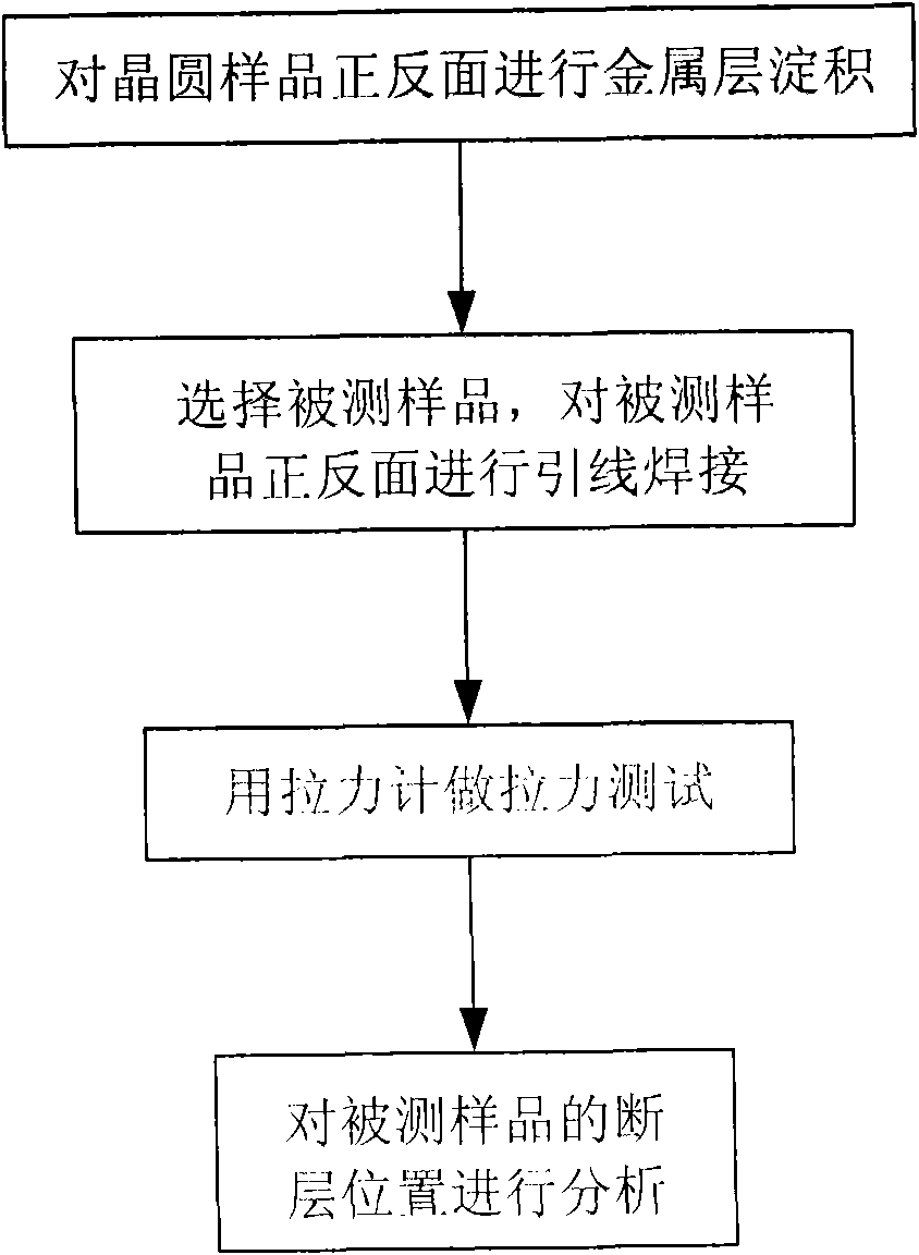
[0023] The following will combine Figure 1 ~ Figure 6 The method for detecting the adhesion of the metal layer on the back of the wafer of the present invention will be further described in detail.

[0024] See figure 1 , The method for detecting adhesion of the metal layer on the back of the wafer of the present invention includes the following steps:

[0025] Step 1. Deposit a metal layer on the front and back of the wafer sample respectively;

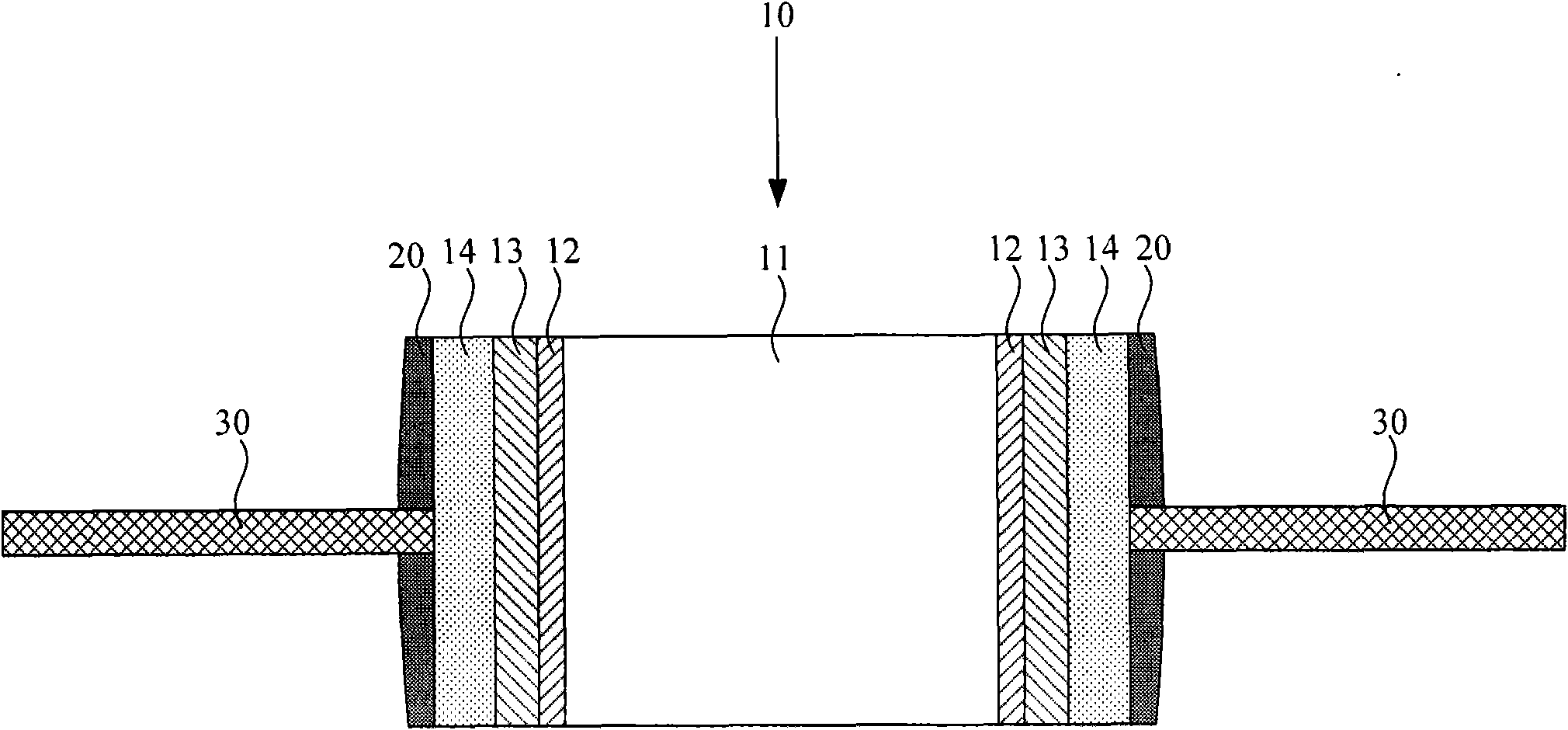
[0026] Step 2: Choose core particles from the wafer samples with metal layers deposited on both the front and back sides as the tested sample, and solder leads on the front and back sides of the tested sample respectively;

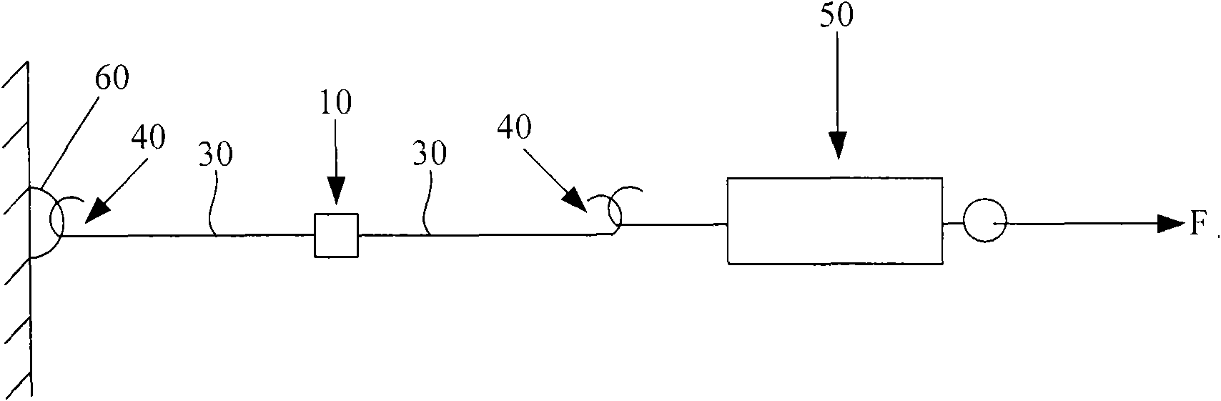
[0027] Step 3: Pull the lead on the back of the tested sample with a tension meter, and record the value of the tensile force before the tested sample is broken;

[0028] Step 4: Analyze the fault location of the tested sample.

[0029] An embodiment is now used to describe in detail the method for detecting the adhesion ...


PUM


Abstract

The invention discloses a method for detecting an adhesive force of a metal layer on the back of a wafer, which comprises the following steps: 1, depositing the metal layer on the front and the back of a wafer sample respectively; 2, selecting a core particle as a detected sample in the wafer sample of which the front and the back are deposited with the metal layers, and welding a lead on the front and the back of the detected sample respectively; 3, pulling the lead on the back of the detected sample by using a tension gauge, and recording a tension value of the detected sample before tension fracture; and 4, analyzing a broken layer position of the detected sample. The method for detecting the adhesive force of the metal layer on the back of the wafer can quantitatively measure the magnitude of the adhesive force of the metal layer on the back of the wafer, is simple and has low cost.

Description

Technical field [0001] The invention relates to a semiconductor manufacturing process, in particular to a method for detecting adhesion of a metal layer on the back of a wafer. Background technique [0002] With the development of semiconductor device packaging technology, it is more and more common to deposit metal layers on the back of the wafer. The adhesion of the metal layer on the back of the wafer to the surface of the wafer is the most critical factor to measure the quality of the metal layer on the back of the wafer. In the manufacturing process of semiconductor devices, the adhesion of the metal layer on the back of the wafer to the surface of the wafer needs to be routinely tested and controlled to ensure the production of high-quality and qualified products. [0003] In the prior art, the method for detecting the adhesion of the metal layer on the back of the wafer is: sticking and dicing the sample to be tested, that is, sticking a blue film on the back of the wafer sa...

Claims


Application Information

Patent Timeline
Patent Type & Authority Applications(China)
IPC IPC(8): H01L21/66
Inventor 傅荣颢刘玮荪
Owner SHANGHAI HUAHONG GRACE SEMICON MFG CORP
Why Eureka
Try Eureka