
Signal-processing board

A signal processing board and signal technology, which is applied in the field of signal processing boards, can solve problems such as difficult fault finding of branch nodes, inability to reconfigure interconnected structures, poor topology flexibility, etc., and achieve good maintainability, good real-time performance, and timing control powerful effect

Active Publication Date: 2013-06-12
BEIJING RUNKE GENERAL TECH
View PDF2 Cites 0 Cited by
  • Summary
  • Abstract
  • Description
  • Claims
  • Application Information

AI Technical Summary

Problems solved by technology

The star structure has the following characteristics: simple structure and control, convenient for network construction and management; its disadvantages are high cost, low reliability, and poor resource sharing ability
The bus structure is to hang each FPGA node on a bus. The characteristics of the bus structure are: simple structure, good expandability, but difficult to maintain and difficult to find faults of branch nodes
Both of the above two interconnection structures have the disadvantage of poor topology flexibility, and the interconnection structure cannot be reconfigured according to specific applications.

Method used


Image

  • Signal-processing board
  • Signal-processing board
  • Signal-processing board

Examples


Embodiment Construction

[0028] The present invention will be described in detail below with reference to the accompanying drawings and in combination with embodiments.

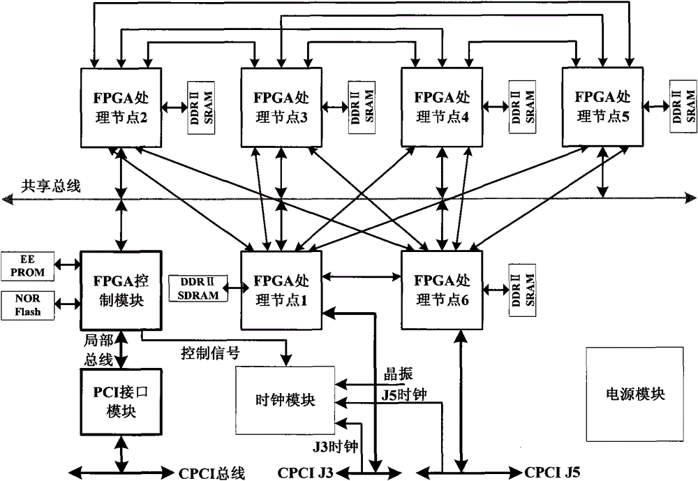
[0029] figure 1 shows a functional block diagram of a signal processing board according to a preferred embodiment of the present invention, as figure 1 As shown, the signal processing board of this embodiment is a multi-FPGA high-speed signal processing board adopting a standard CPCI bus structure, which includes: a power supply module, a clock module, six FPGA processing nodes, an FPGA master control module and a PCI interface module.

[0030] The signal processing board adopts a full FPGA structure, using seven FPGA chips in total, one of which is used as the FPGA main control module, and the FPGA main control module is the main control device of the entire signal board. Its functions include: (1) PCI timing interface , to achieve PCI slave mode and PCI master mode access; (2) each FPGA processing node configuration interface, to...


PUM


Abstract

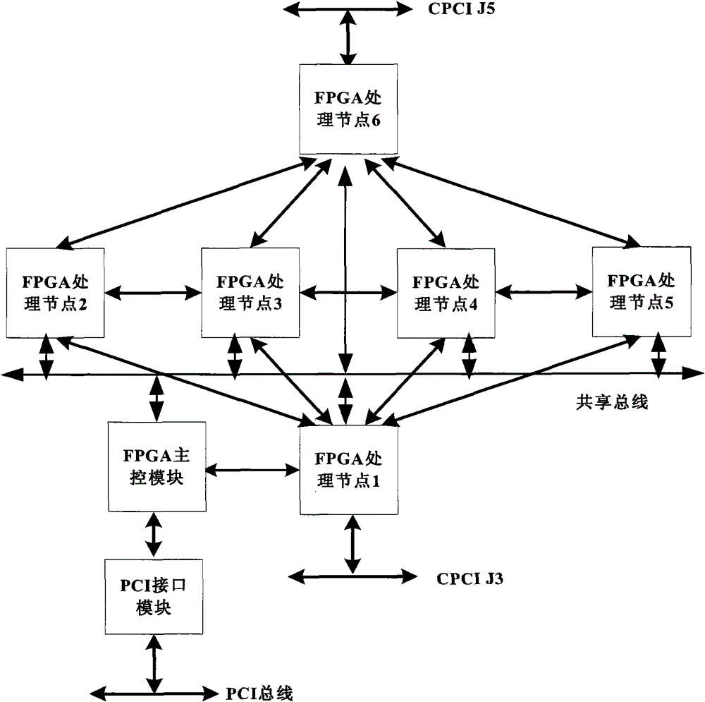
The invention provides a signal-processing board, which comprises a plurality of FPGA processing nodes, an FPGA main control module, a PCI interface module, a clock module and a power supply module, wherein the plurality of FPGA processing nodes are interconnected by an interconnection bus in a totally communicated topological structure and the interconnection bus is used for transmitting a high-speed data signal; the FPGA main control module is interconnected with the plurality of FPGA processing nodes through a shared bus which is used for transmitting a control signal; the PCI interface module is connected with the FPGA main control module through a local bus; the clock module is connected with the FPGA main control module, controlled by the main control module and used for supplying aworking clock to the signal-processing board; and the power supply module is used for supplying a voltage required by the signal-processing board. The topological structure of the plurality of FPGA processing nodes of the signal-processing board is flexible and the reconfiguration of the interconnection structure can be implemented according to specific application.

Description

technical field [0001] The invention relates to the field of digital signal processing, in particular to a signal processing board. Background technique [0002] In the field of digital signal processing, the traditional division method is: a dedicated DSP (Digital Signal Processing, digital signal processor) chip is low in cost, flexible in algorithm, and powerful in function. It is a general signal processor and is mainly used for data calculation; FPGA (Field Programmable Gate Array, Field Programmable Gate Array) chips have good real-time performance and strong timing control capabilities, and are mostly used for system control. [0003] Because DSP uses software to realize data processing, it may not be able to meet the application requirements in occasions with large data throughput and high real-time requirements. With the development of FPGA technology, the interface and algorithm resources in FPGA are becoming more and more abundant, and FPGA is gradually penetrati...

Claims


Application Information

Patent Timeline
Patent Type & Authority Patents(China)
IPC IPC(8): G06F13/40
Inventor 江培华赖永青陶青长王胜勇
Owner BEIJING RUNKE GENERAL TECH
Learn More