Supercharge Your Innovation With Domain-Expert AI Agents!

TFT-LCD (Thin Film Transistor Liquid Crystal Display) array substrate and manufacturing method thereof, as well as liquid crystal display panel

An array substrate and substrate technology, which is applied in semiconductor/solid-state device manufacturing, static indicators, optics, etc., and can solve the problems of sudden changes in image brightness, voltage drop, and poor screen display.

Active Publication Date: 2013-05-22
BOE TECH GRP CO LTD +1
View PDF0 Cites 2 Cited by
  • Summary
  • Abstract
  • Description
  • Claims
  • Application Information

AI Technical Summary

Problems solved by technology

The presence of feedthrough voltage will cause the voltage applied to the pixel electrode to drop
[0004] The inversion of the liquid crystal molecules is realized by the voltage difference between the pixel electrode and the common electrode, and in order to delay the aging of the liquid crystal molecules, the voltage difference on both sides of the liquid crystal molecules in adjacent frames is opposite, and the pixel electrode voltage drops, which will cause When LCD is displayed, the brightness of the image between adjacent frames changes abruptly
like Figure 16 Shown is a schematic diagram of the feedthrough voltage generated on the pixel electrode of the TFT-LCD array substrate in the prior art. In the nth frame of liquid crystal display time, the signal 11 input to the gate electrode at the initial stage is at a high level, and the TFT in the pixel area Open, the signal 12 input in the data line is input to the pixel electrode through the TFT, the voltage of the signal 13 input on the pixel electrode is greater than the voltage of the signal 14 input on the common electrode, due to the feedthrough, the signal 13 input on the pixel electrode and the data Compared with the signal 12 input in the line, the voltage difference between the signal 13 input on the pixel electrode and the signal 14 input on the common electrode is smaller than the expected voltage difference, that is, the voltage difference applied to both sides of the liquid crystal molecule will be less than Expected voltage difference; in the n+1th frame of liquid crystal display time, the signal 11 input to the gate electrode at the initial stage is high level, the TFT in the pixel area is turned on, and the signal 12 input in the data line is input to the pixel electrode through the TFT , the voltage of the signal 13 input on the pixel electrode is lower than the voltage of the signal 14 input on the common electrode, due to feedthrough, the signal 13 input on the pixel electrode is lower than the signal 12 input in the data line, and the input signal 12 on the pixel electrode The voltage difference between the signal 13 and the signal 14 input on the common electrode is greater than the expected voltage difference, that is, the voltage difference applied to both sides of the liquid crystal molecules will be greater than the expected voltage difference, so the two adjacent frames of liquid crystal display time are applied to the The voltage difference between the two sides of the liquid crystal molecules will have a sudden change, resulting in poor picture display

Method used


Image

  • TFT-LCD (Thin Film Transistor Liquid Crystal Display) array substrate and manufacturing method thereof, as well as liquid crystal display panel
  • TFT-LCD (Thin Film Transistor Liquid Crystal Display) array substrate and manufacturing method thereof, as well as liquid crystal display panel
  • TFT-LCD (Thin Film Transistor Liquid Crystal Display) array substrate and manufacturing method thereof, as well as liquid crystal display panel

Examples


Embodiment Construction

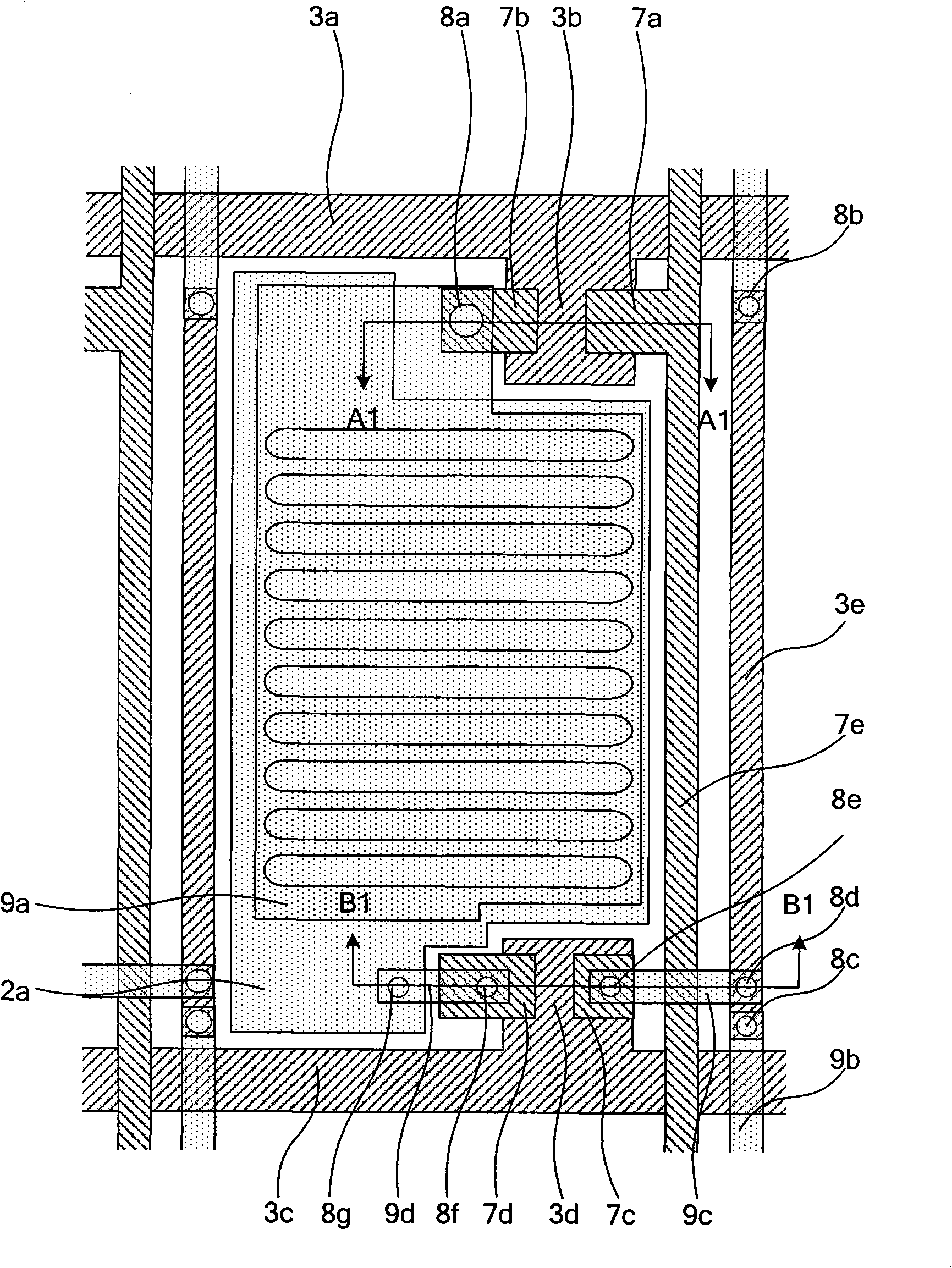
[0043]The TFT-LCD array substrate provided by the present invention includes a first gate line and a first data line, a first electrode and a first TFT are formed in the pixel area defined by the first gate line and the first data line, and a second TFT and The second electrode, the second TFT is connected to the second electrode, the first electrode and the second electrode are used to form a voltage difference to drive the liquid crystal molecules to reverse, and the first TFT and the second TFT are turned on or off at the same time.

[0044] The technical solutions of the present invention will be described in further detail below with reference to the accompanying drawings and embodiments.

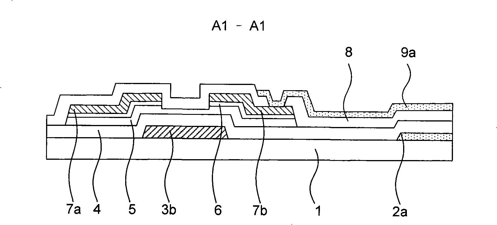
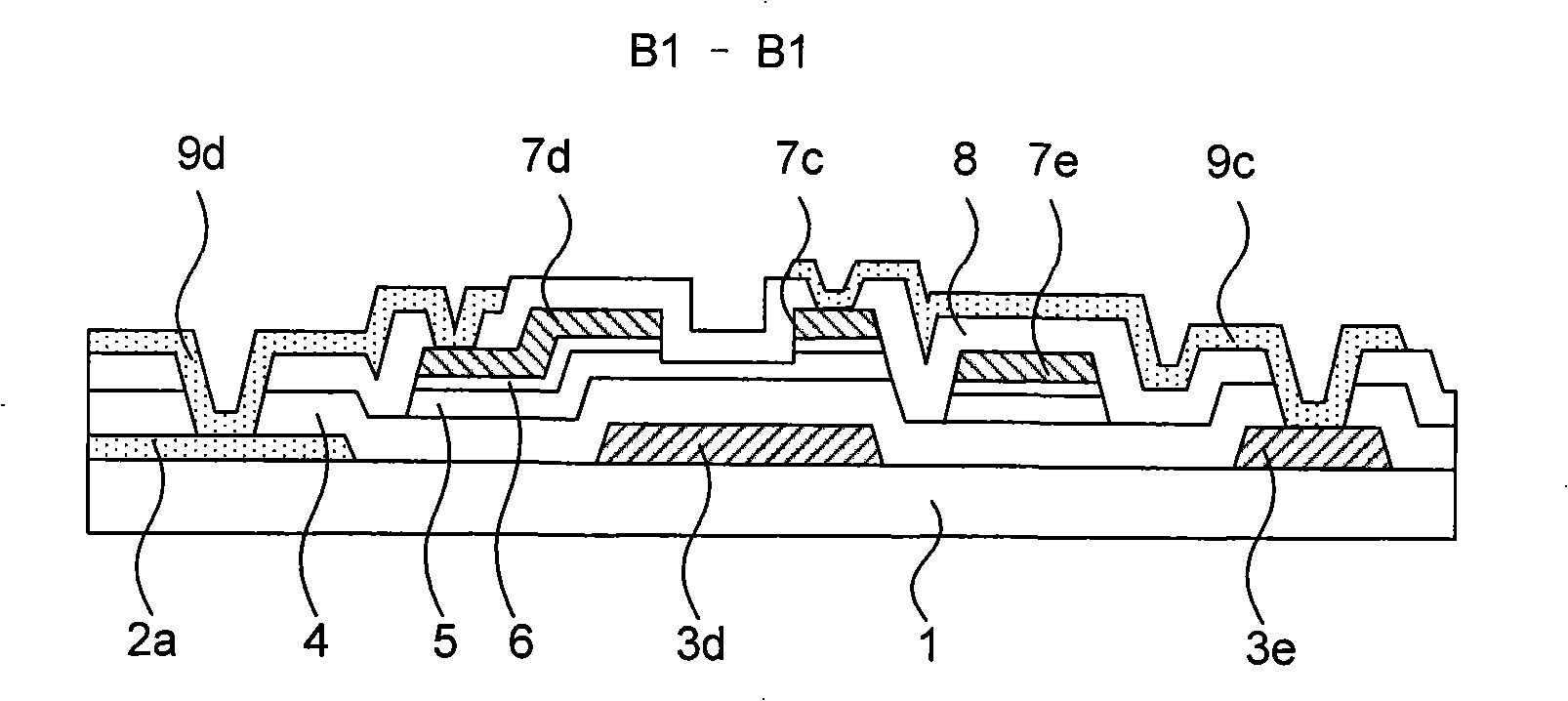
[0045] Figure 1a It is a plan view of the first embodiment of the TFT-LCD array substrate of the present invention, Figure 1b for Figure 1a The cross-sectional view of A1-A1 in the middle, Figure 1c for Figure 1a Sectional view of B1-B1 direction in the middle. Such as Figu...


PUM

PropertyMeasurementUnit
thicknessaaaaaaaaaa
thicknessaaaaaaaaaa

Abstract

A TFT-LCD array substrate, a manufacturing method thereof and a liquid crystal display panel are provided in the invention. The TFT-LCD array substrate comprises a plurality of first gate lines and a plurality of first data lines, and a plurality of pixel regions are defined by intersecting the first gate lines and the first data lines with each other. A first pixel electrode and a first TFT are formed in each of the pixel regions, and a second TFT and a second pixel electrode are further comprised in each of the pixel regions. The second TFT is connected with the second pixel electrode, the first pixel electrode and the second pixel electrode form the voltage difference to drive the reversion of the liquid crystal molecules, and the first TFT and the second TFT are turned on or off simultaneously.

Description

technical field [0001] The invention relates to a liquid crystal display and a manufacturing method, in particular to a thin film transistor liquid crystal display (TFT-LCD) array substrate, a manufacturing method thereof and a liquid crystal display panel. Background technique [0002] In the TFT-LCD array substrate, a layer of transparent conductive film is usually deposited on the transparent substrate as the common electrode, and then the pixel electrode is formed on the substrate. The electric field generated between the pixel electrode and the common electrode parallel to the transparent substrate makes the liquid crystal molecules Rotating in a plane parallel to the transparent substrate, the non-overlapping part between the pixel electrode and the common electrode forms a liquid crystal capacitor; the overlapping part between the pixel electrode and the common electrode forms a storage capacitor for maintaining the voltage on the pixel electrode. [0003] In the proc...

Claims


Application Information

Patent Timeline
Patent Type & Authority Patents(China)
IPC IPC(8): G02F1/1362H01L27/12H01L21/84
CPCG09G2320/0247H01L27/1214G09G2300/0434G02F2001/134318G02F2201/50G09G2300/0823G02F1/13624G09G2320/0219H01L27/12G09G3/3614G09G3/3648G02F1/134318H01L27/124
Inventor 赵鑫明星周伟峰张文余郭建
Owner BOE TECH GRP CO LTD
Features
  • R&D
  • Intellectual Property
  • Life Sciences
  • Materials
  • Tech Scout
  • Unparalleled Data Quality
  • Higher Quality Content
  • 60% Fewer Hallucinations
Learn More