On-line detection method and system for wafer

A wafer and inspection station technology, applied in the field of wafer online inspection methods and systems, can solve problems such as delaying product time, reducing inspection effects, and failing to make full use of inspection station inspection capabilities, so as to improve rationality and prevent product production time. Effect

Active Publication Date: 2010-10-27
SEMICON MFG INT (SHANGHAI) CORP
View PDF0 Cites 17 Cited by
  • Summary
  • Abstract
  • Description
  • Claims
  • Application Information

AI Technical Summary

Problems solved by technology

[0007] The problem to be solved by the present invention is to provide a method and system for on-line inspection of wafers, so as to avoid the possible prob...

Method used


Image

  • On-line detection method and system for wafer
  • On-line detection method and system for wafer
  • On-line detection method and system for wafer

Examples


Embodiment approach

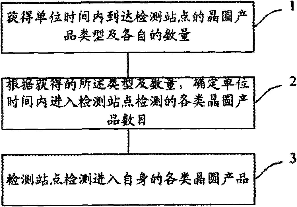
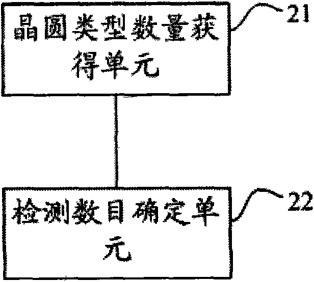
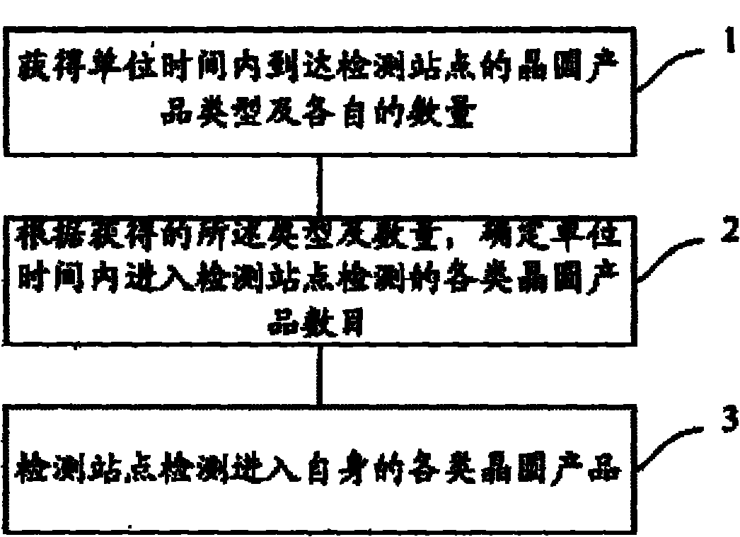
[0018] First, obtain the type of wafer product that arrives at the inspection site from the dispatch order, which is a well-known term in the art, including the type of product produced, and information such as which stations each product needs to pass through; then for various wafer products , respectively perform the following operations a1 to a3 until the number of all types of wafer products arriving at the inspection site is calculated:

[0019] a1, determine the processing sites that this type of wafer products need to pass through before the testing site;

[0020] a2, add up the time it takes for each processing site to process the wafer product in process and the time for the wafer product in process to wait for processing before the processing site;

[0021] In step a2, obtaining the time that the wafer product waits for processing before the processing site can also be realized in a variety of ways, preferably in this embodiment, it also includes determining the wait...


PUM


Abstract

The invention provides an on-line detection method and an on-line detection system for a wafer, which avoid the problems that the conventional detection scheme possibly delays product time, reduces the detection effect and cannot make full use of the detection capability of a detection site. The method comprises the following steps of: acquiring types and numbers of wafer products reaching the detection site in unit time; determining the number of various wafer products detected in the detection site in unit time according to the acquired types and the acquired numbers; and detecting the various wafer products entering the detection site by the detection site.

Description

technical field [0001] The invention relates to the field of semiconductor manufacturing, in particular to a wafer on-line detection method and system. Background technique [0002] In the process of semiconductor manufacturing, wafers are sequentially processed by a series of processing stations, and finally semiconductor products are formed. The processing stations include one or more processing machines, and the wafers are processed by the machines. There is an inspection station between the processing stations to inspect some of the wafers processed before the inspection station. Since this inspection is carried out during the product production process, it is called on-line inspection. The number of wafers that enter the inspection station for inspection can vary. It is pre-set that the number must be less than or equal to the throughput of the inspection site, that is, the maximum number of wafers that the inspection site can inspect per unit time. [0003] The indust...

Claims


Application Information

Patent Timeline
IPC IPC(8): H01L21/00H01L21/66
Inventor 杨健孙强陈思安吕秋玲
Owner SEMICON MFG INT (SHANGHAI) CORP
Why Eureka
Try Eureka