Printed circuit board

A technology of printed circuit boards and substrates, which is applied to printed circuit components, electrical connection printed components, etc., can solve problems such as increasing the firmness of wire welding, and achieve the effect of protecting reliability

Inactive Publication Date: 2010-10-27
OCEANS KING LIGHTING SCI&TECH CO LTD +1
View PDF4 Cites 2 Cited by
  • Summary
  • Abstract
  • Description
  • Claims
  • Application Information

AI Technical Summary

Problems solved by technology

However, sometimes due to installation and other issues, only one side of the printed circuit board is required to have solder joints, and the other side must be completely insulated. At this time, this method cannot be used to increase the firmness of wire welding.

Method used


Image

  • Printed circuit board
  • Printed circuit board
  • Printed circuit board

Examples


Embodiment Construction

[0023] The preferred embodiments of the present invention will be described in detail below with reference to the drawings.

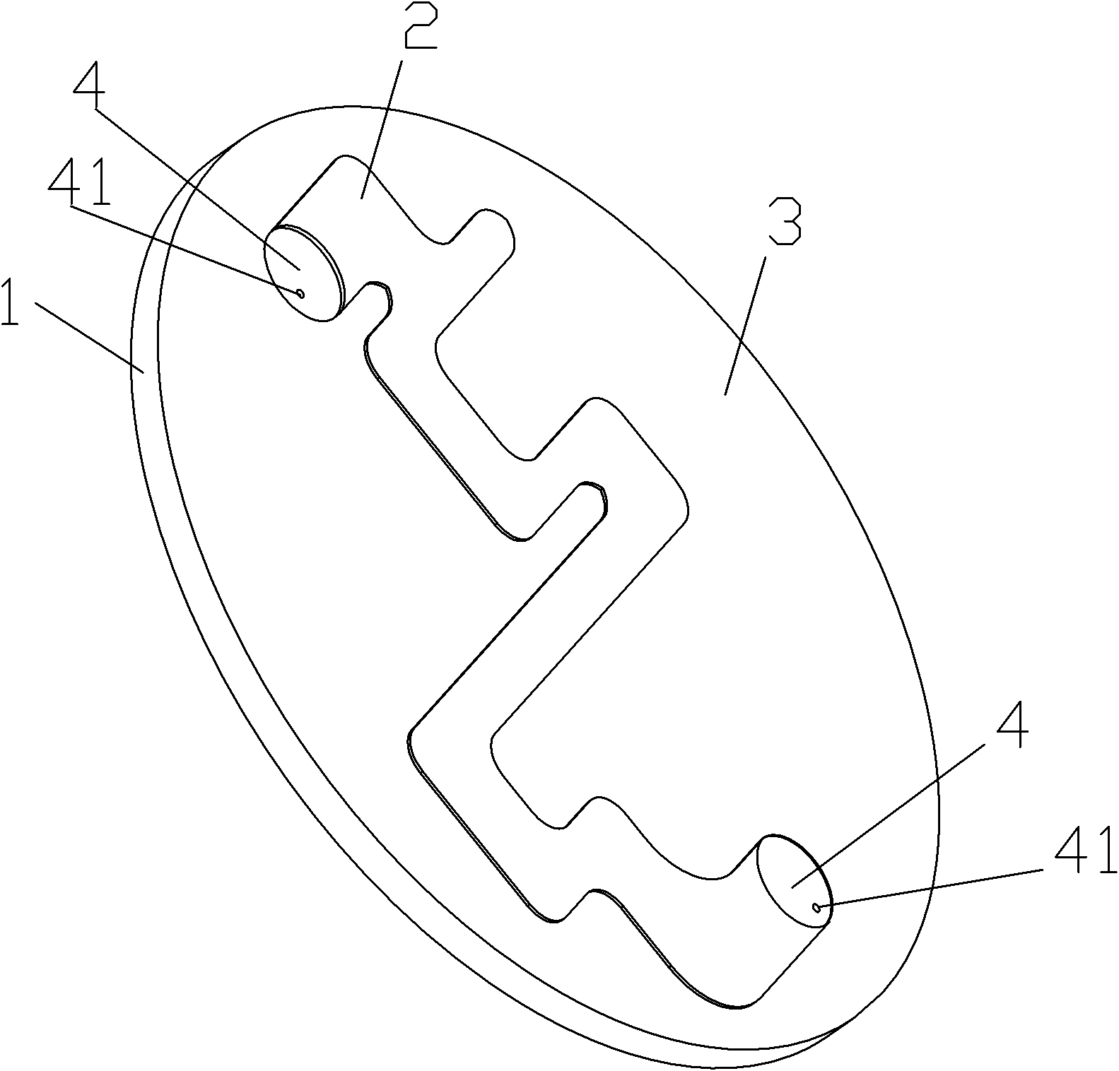
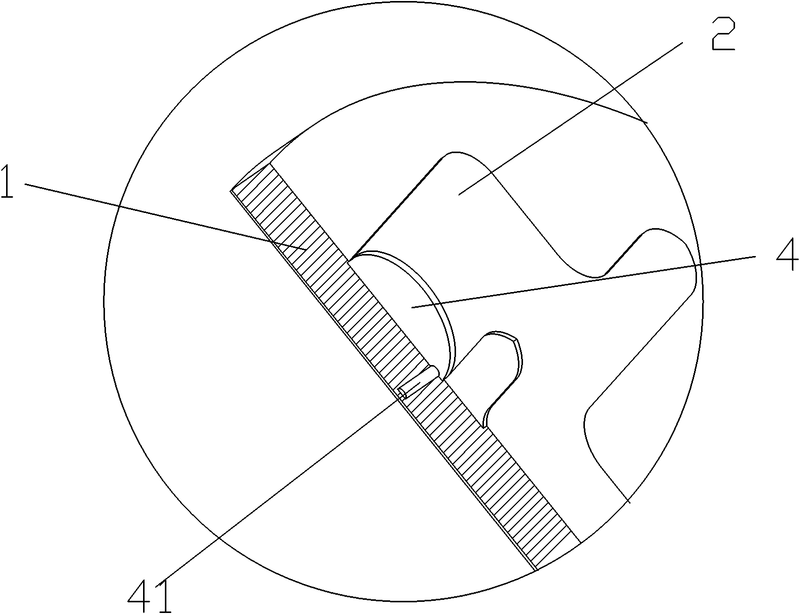
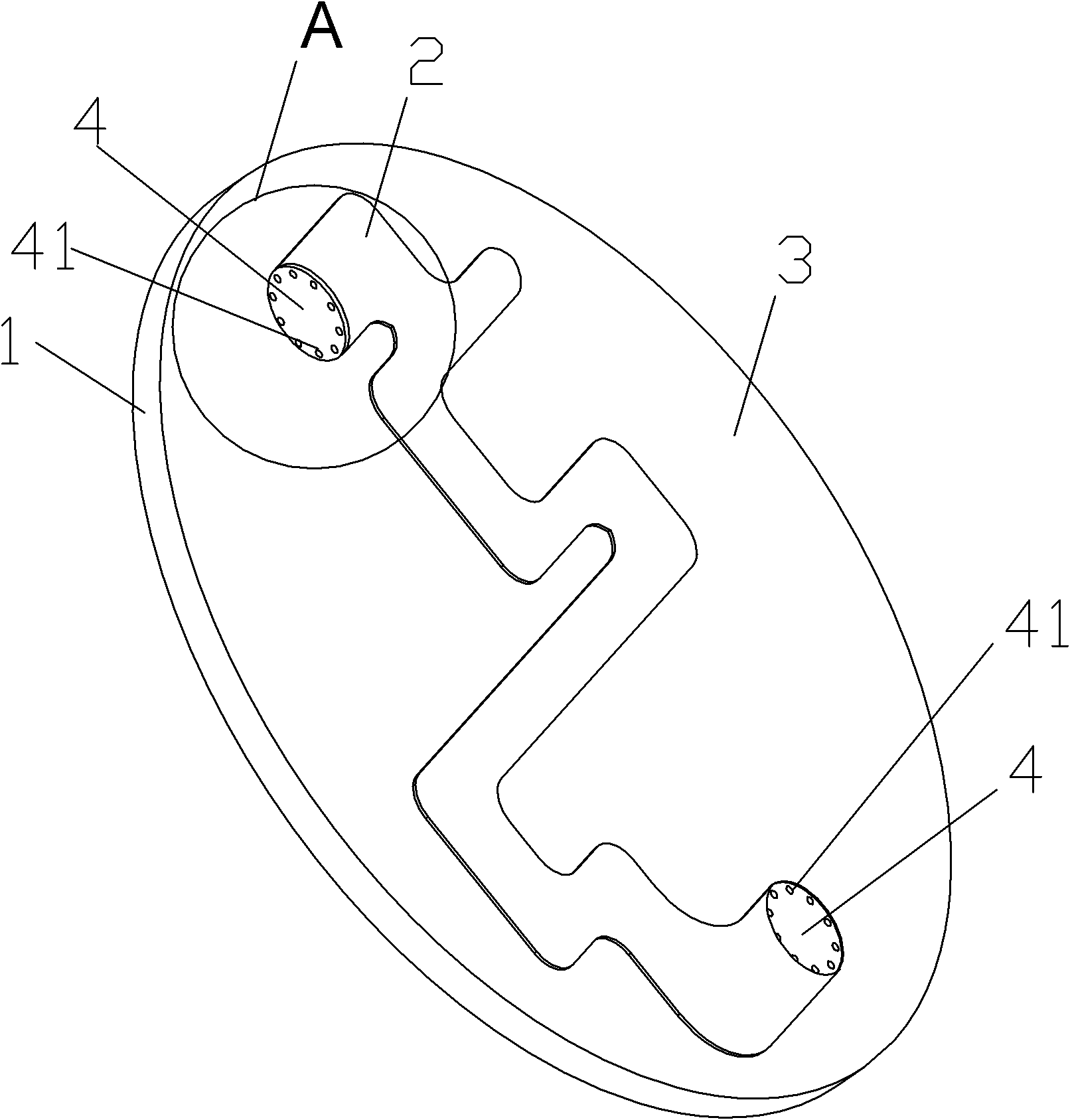
[0024] The schematic diagram of the printed circuit board structure of the preferred embodiment of the present invention is as figure 1 shown, see also figure 2 , which includes a substrate 1, a copper skin 2 laid on the front of the substrate 1, and a front insulating layer 3, the front insulating layer 3 is pressed outside the copper skin 2, and at least one exposed copper area 4 is left. A hole 41 is provided along the thickness direction of the substrate 1 in the exposed copper area 4 , and a copper skin 2 is attached to the inner wall of the hole 41 . By setting the hole 41 along the thickness direction of the substrate 1 in the exposed copper area 4 of the printed circuit board, and laying the copper skin 2 on the inner wall of the hole 41, the solder joint of the wire in the exposed copper area 4 is like a hand firmly grasping Like the substra...


PUM


Abstract

The invention relates to a printed circuit board. The printed circuit board comprises a substrate, a copper sheet laid on the front surface of the substrate, and a front-surface insulating layer which is pressed outside the copper sheet and provided with a copper-exposed region, wherein the copper-exposed region is provided with holes along a thickness direction of the substrate, and the copper sheet in the copper-exposed region extends to the inside walls of the holes. The copper-exposed region of the printed circuit board is provided with the holes along the thickness direction of the substrate, and the copper sheet is laid on the inside walls of the holes, so that solder joints in the copper-exposed region grasp the substrate tightly as a hand; when the copper sheet at the solder joints is peeled off or torn down from the substrate, a wire soldered in the copper-exposed region overcomes adhesive forces in horizontal and vertical directions, and also overcomes an additional adhesiveforce due to the area increase of the laid copper sheet; therefore, the reliability of the printed circuit board can be protected effectively.

Description

technical field [0001] The invention relates to a printed circuit board structure, in particular to a printed circuit board capable of resisting the tearing of the copper skin by the wire and preventing the copper skin from falling off the substrate. Background technique [0002] Ordinary printed circuit boards include a substrate, a copper skin and an insulating layer, wherein a copper skin for conducting electricity is applied on the substrate, and an insulating layer is pressed on the copper skin. The insulating layer can not only be used for insulation, but also protect the copper skin on the substrate. role. [0003] According to the circuit design, there are often several exposed copper areas for soldering wires on the printed circuit board, that is, the end of the copper wires. The wire is welded on the exposed copper area by soldering tin, so as to be electrically connected with the printed circuit board. [0004] When selecting a wire, if the required current flow...

Claims


Application Information

Patent Timeline
Patent Type & Authority Applications(China)
IPC IPC(8): H05K1/11H05K1/02
Inventor 周明杰刘廷明
Owner OCEANS KING LIGHTING SCI&TECH CO LTD
Why Eureka
Try Eureka