Display device, array substrate and manufacturing method

A technology of an array substrate and a manufacturing method, applied in the field of liquid crystal displays, can solve problems such as reliability decline and semiconductor layer damage, and achieve the effects of improving reliability and avoiding damage

Inactive Publication Date: 2017-07-28
SHENZHEN CHINA STAR OPTOELECTRONICS SEMICON DISPLAY TECH CO LTD
View PDF2 Cites 4 Cited by
  • Summary
  • Abstract
  • Description
  • Claims
  • Application Information

AI Technical Summary

Problems solved by technology

[0004] The present invention mainly provides a display device, an array substrate and a manufacturing method thereof, so as to solve the problem in the prior art that the semiconductor layer is easily damaged when the gate insulating layer is manufactured, which leads to a decrease in the reliability of the TFT.

Method used


Image

  • Display device, array substrate and manufacturing method
  • Display device, array substrate and manufacturing method
  • Display device, array substrate and manufacturing method

Examples


Embodiment 1

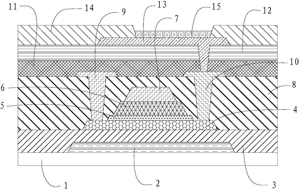
[0029] see figure 1 , figure 1 It is a schematic diagram of the mechanism after the formation of the pixel definition layer 14 and the arrangement of the organic light emitting diodes 15 in an array substrate manufacturing method of the present invention. from figure 1 It can be seen that an array substrate in this embodiment includes:

[0030] A light-shielding layer 2, a barrier layer 3, and a semiconductor layer 4 are sequentially formed on the base substrate 1 from bottom to top;

[0031] a first gate insulating layer 5, formed on one side of the semiconductor layer 4, and formed by a first method;

[0032] The second gate insulating layer 6 is formed on the side of the first gate insulating layer 5 facing away from the semiconductor layer 4, and is formed by a second method;

[0033] Wherein, the first method can protect the reliability of the semiconductor layer 4 .

[0034] In this embodiment, the array substrate of the present invention further includes a gate 7 f...

Embodiment 2

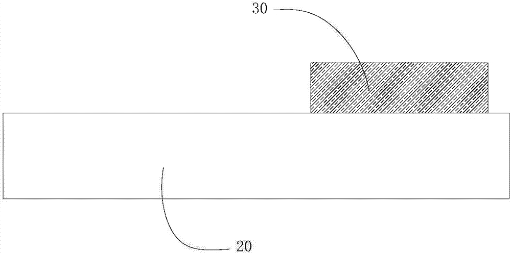
[0041] This embodiment provides a display device, which includes the array substrate 20 described in Embodiment 1, on which a corresponding driving circuit 30 is disposed. Since the array substrate 20 has been described in detail in the first embodiment, it will not be repeated here.

[0042] In a display device of the present invention, the array substrate 20 is deposited to form the first gate insulating layer 5 by atomic deposition, and the second gate insulating layer 6 is deposited by chemical vapor deposition to avoid damage to the semiconductor layer 4, Improving the reliability of thin film transistors and reducing the influence of atomic deposition on production efficiency due to low deposition rate can achieve a good balance between production efficiency and TFT reliability.

Embodiment 3

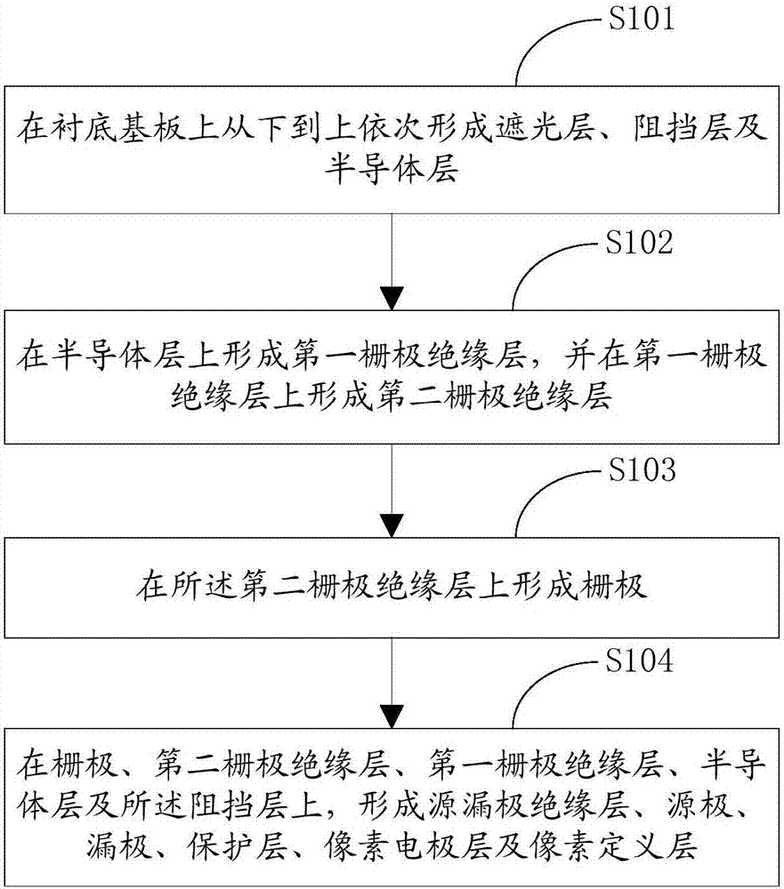
[0044] see image 3 , image 3 It is a flow chart of the overall implementation steps of a method for fabricating an array substrate in this embodiment. from image 3 It can be seen that a method for manufacturing an array substrate in this embodiment includes the following steps:

[0045] Step S101 : Forming a light-shielding layer 2 , a barrier layer 3 and a semiconductor layer 4 sequentially from bottom to top on the base substrate 1 . like Figure 4 as shown, Figure 4 It is a schematic diagram of the structure when the light shielding layer 2 , the blocking layer 3 and the semiconductor layer 4 are sequentially formed on the base substrate 1 in a method for fabricating an array substrate in this embodiment.

[0046] Step S102 : forming a first gate insulating layer 5 on the semiconductor layer 4 , and forming a second gate insulating layer 6 on the first gate insulating layer 5 .

[0047] In this step, the first gate insulating layer 5 is formed on one side of the s...


PUM


Abstract

The invention discloses a display device, an array substrate and a manufacturing method. The array substrate comprises a semiconductor layer, a first grid insulation layer and a second grid insulation layer. The first grid insulation layer is formed on one face of the semiconductor layer by use of a first method. The second grid insulation layer is formed on one side, opposite to semiconductor layer, of the first grid insulation layer by use of a second method. By use of the first method, reliability of the semiconductor layer can be protected. Thus, the semiconductor layer is prevented from being damaged and reliability of a thin film transistor is improved.

Description

technical field [0001] The invention relates to the field of liquid crystal displays, in particular to a display device, an array substrate and a manufacturing method thereof. Background technique [0002] Thin Film Transistor Liquid Crystal Display (TFT-LCD for short) is an important flat-panel display device. Its main structure is an array substrate and a color filter substrate arranged in a pair of boxes, and filled in the array substrate and color filter substrate. between the liquid crystal layers. Gate lines and data lines and pixel units defined by the gate lines and data lines are formed on the array substrate, and each pixel unit includes a thin film transistor (Thin Film Transistor, TFT for short) and a pixel electrode. During the display process, the TFT is used as a switch to control the application of a driving electric field to the liquid crystal, thereby controlling the rotation of the liquid crystal and realizing the display of the screen. Usually, a black ...

Claims


Application Information

Patent Timeline
Patent Type & Authority Applications(China)
IPC IPC(8): H01L27/12H01L29/786H01L29/51H01L21/77
Inventor 刘兆松
Owner SHENZHEN CHINA STAR OPTOELECTRONICS SEMICON DISPLAY TECH CO LTD
Why Eureka
Try Eureka