Optical touch panel structure

A touch panel, optical technology, applied in the direction of instruments, electrical digital data processing, input/output process of data processing, etc., can solve problems such as color deviation

Inactive Publication Date: 2010-12-01
HANNSTAR DISPLAY CORPORATION
View PDF0 Cites 29 Cited by
  • Summary
  • Abstract
  • Description
  • Claims
  • Application Information

AI Technical Summary

Problems solved by technology

However, although this method can avoid sacrificing too much panel brightness, it will cause serious color deviation due to the low aperture ratio of the blue area, especially on some high-resolution panels.
[0005] In view of this, the present invention proposes an optical touch panel structure to solve the problem of color deviation

Method used


Image

  • Optical touch panel structure
  • Optical touch panel structure
  • Optical touch panel structure

Examples


Embodiment Construction

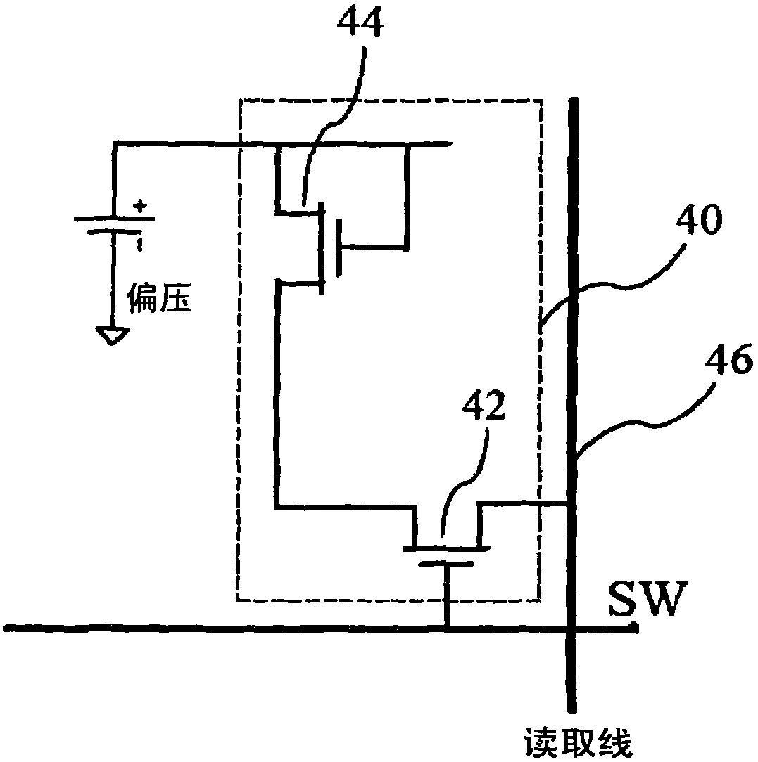
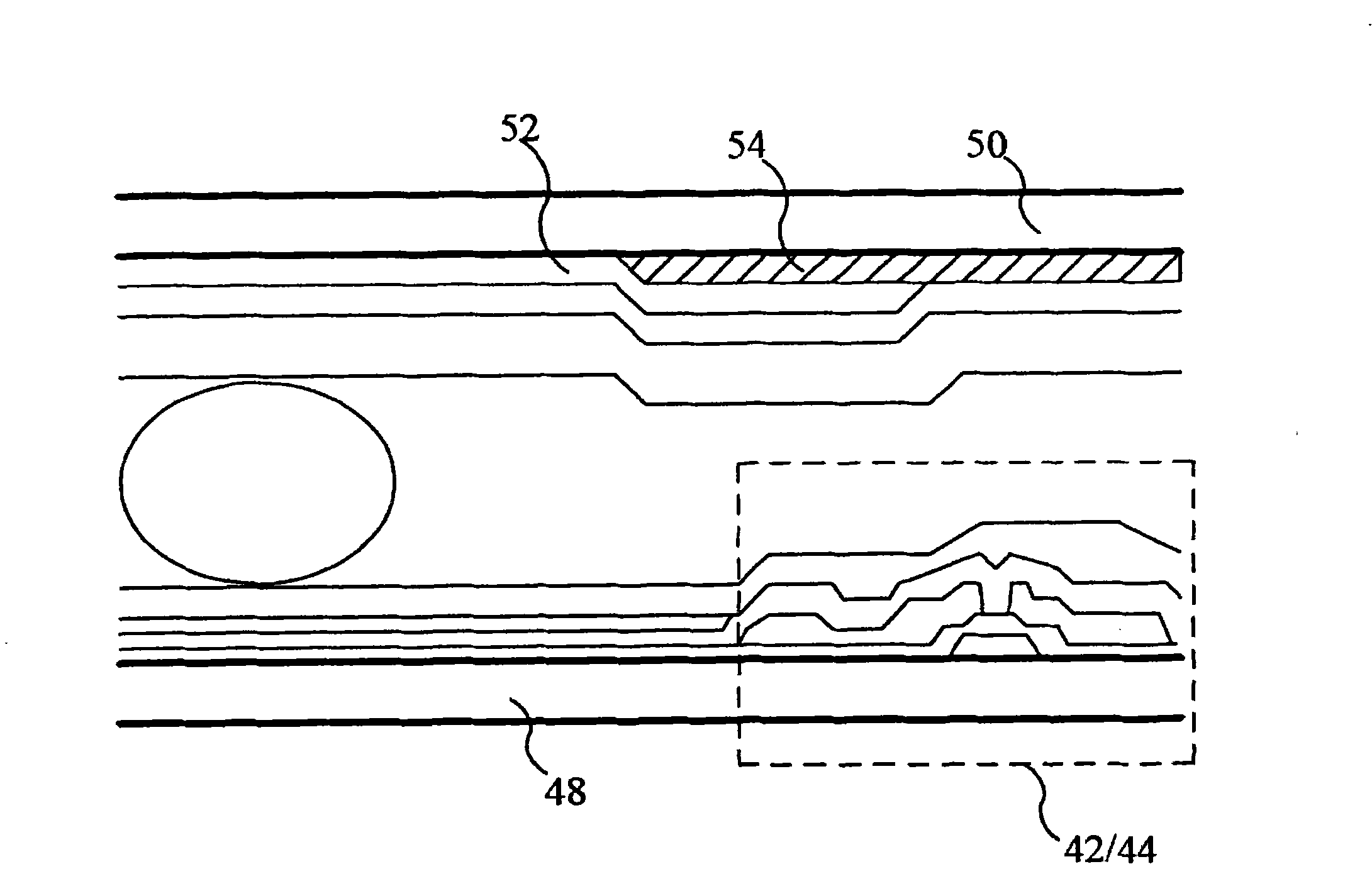
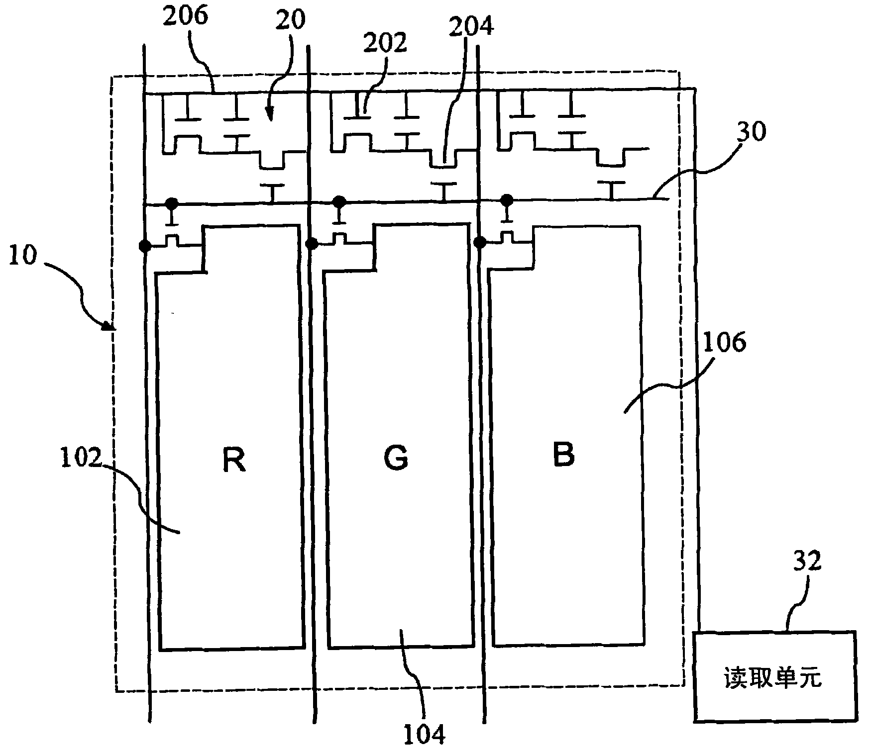
[0035] The present invention utilizes the differences in the aperture ratios occupied by the red, green and blue blocks by disposing photosensitive elements in the red, green and blue blocks to adjust the aperture ratios of the red, green and blue blocks, so that the brightness and The color deviation reaches a balance point to solve the problem that the color deviation easily occurs in the prior art.

[0036] An optical touch panel structure includes a thin film transistor substrate, a color filter substrate, and a liquid crystal layer sandwiched by the two substrates. The thin film transistor substrate is provided with a plurality of photosensitive elements; the color filter substrate has a plurality of pixel units, and a black matrix is ​​respectively arranged on each pixel unit and corresponding to the photosensitive element, and each pixel unit includes a red block, The green block and the blue block, among which the opening rate of the green block is the largest. The pr...


PUM


Abstract

The invention discloses an optical touch panel structure, comprising a color filter substrate with multiple pixel units and a thin film transistor substrate, wherein each pixel unit is composed of a red block, a green block and a blue block; the thin film transistor substrate is provided with multiple photo-sensitive cells corresponding to the pixel units; the non-photo-sensitive areas corresponding to the photo-sensitive cells on the pixel units are provided with a black matrix respectively; the black matrixes are configured on the red block or the green block or the blue block so as to adjust the aperture opening ratio of the red block, the green block and the blue block by utilizing the occupied area of the black matrix on each block and enable the deviations of brightness and color to reach a balance point respectively, thus minimizing the color deviation and brightness loss.

Description

technical field [0001] The invention relates to a touch display device, in particular to an optical touch panel structure with a photosensitive thin film transistor. Background technique [0002] In recent years, touch panels have been widely used, and there are many types, among which the in-cell touch panel, which directly integrates the touch function into the display panel, has attracted the most attention. [0003] At present, most of the in-cell touch panels are optical sensing, which uses a photo sensor embedded in the display panel to detect the change of photocurrent to determine the touch position event. These photosensors can be thin film transistor (TFT) sensors 40, such as figure 1 As shown, it is composed of a switch transistor (SW TFT) 42 and a photosensitive transistor 44 (Photo TFT); when the switch transistor 42 is turned on, the photocurrent signal generated by the photosensitive transistor 44 will pass through the reading line 46, and when the light inte...

Claims


Application Information

Patent Timeline
Patent Type & Authority Applications(China)
IPC IPC(8): G02F1/133G06F3/042
Inventor 蔡正晔陈威州陈柏仰
Owner HANNSTAR DISPLAY CORPORATION
Why Eureka
Try Eureka