Method for measuring expansion and shrinkage of printed circuit board, and printed circuit board

A printed circuit board, expansion and shrinkage measurement technology, applied in printed circuit parts, measuring devices, instruments, etc., can solve the problems of circuit board defects, scrap, expansion and shrinkage, etc., and achieve the effect of improving circuit board defects and reducing scrap rate.

Inactive Publication Date: 2010-12-08
APCB ELECTRONICS SHENZHEN CO LTD
View PDF8 Cites 12 Cited by
  • Summary
  • Abstract
  • Description
  • Claims
  • Application Information

AI Technical Summary

Problems solved by technology

However, when the inner boards are pressed together, one or more layers of the inner boards will expand and shrink, resulting in defective or even scrapped circuit boards.
[0003] see figure 1 , the existing technology generally adopts a circular test point at the corresponding position of the four corners of each inner layer board. After the circuit board is pressed, these circular test points will form a concentric ring. Then, according to the concentric ring The distance between the ring and the ring, check whether the inner layer board is deflected and expands and shrinks, so as to detect which layer of the inner layer board has expanded and shrunk, but this method cannot actually measure the actual expansion and contraction of each inner layer board Therefore, this method cannot provide data support for subsequent changes in inner layer film compensation
[0004] Therefore, the expansion and contraction measurement technology of the existing circuit board still needs to be improved and improved.

Method used


Image

  • Method for measuring expansion and shrinkage of printed circuit board, and printed circuit board
  • Method for measuring expansion and shrinkage of printed circuit board, and printed circuit board
  • Method for measuring expansion and shrinkage of printed circuit board, and printed circuit board

Examples


Embodiment Construction

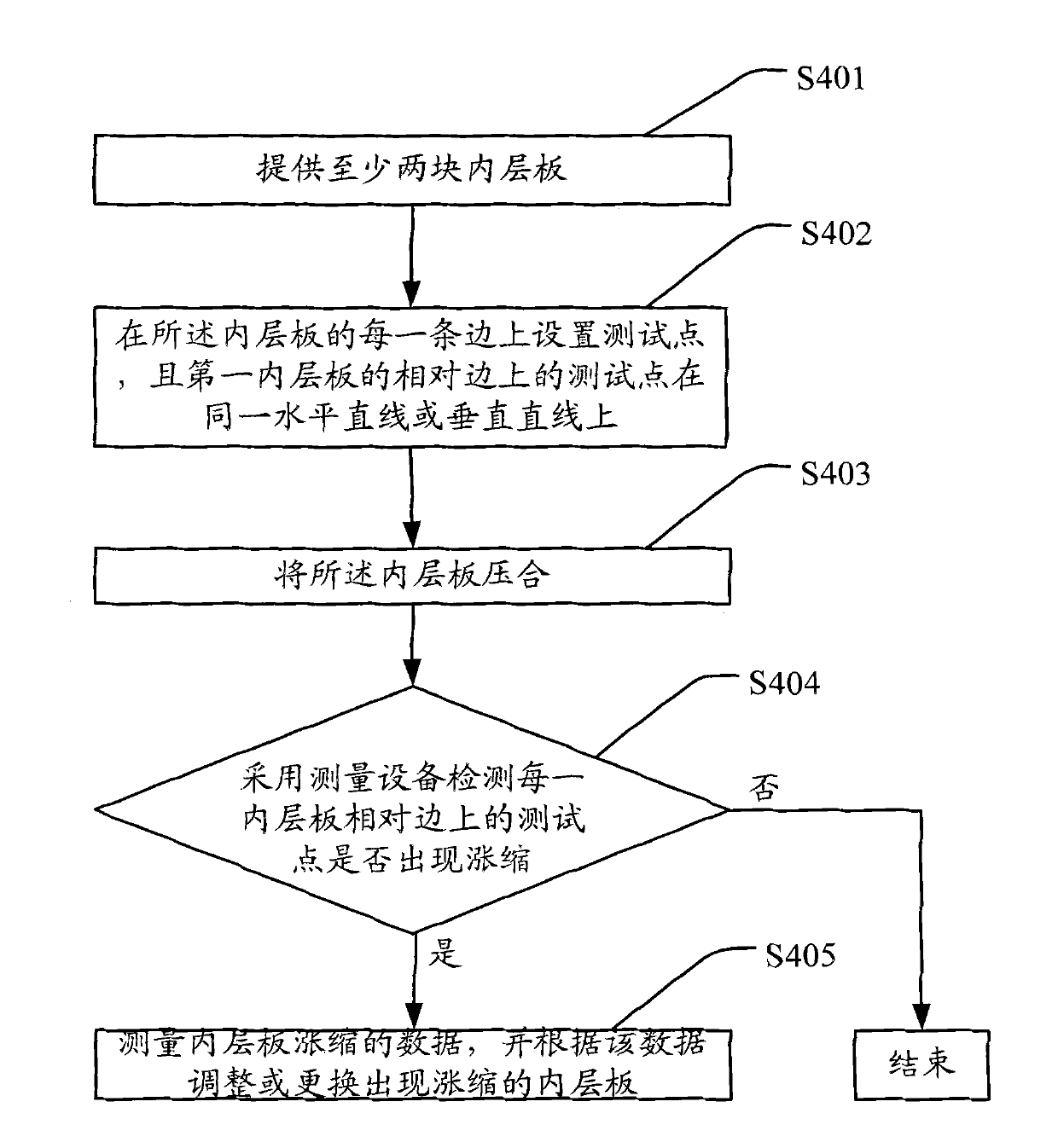
[0030] The present invention provides a method for measuring the expansion and shrinkage of printed circuit boards and printed circuit boards. In order to make the purpose, technical solution and effect of the present invention clearer and clearer, the present invention will be further described in detail below with reference to the accompanying drawings and examples. It should be understood that the specific embodiments described here are only used to explain the present invention, not to limit the present invention.

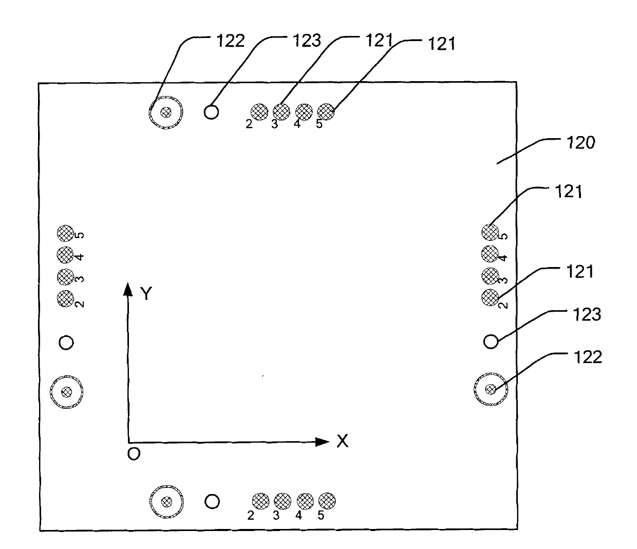
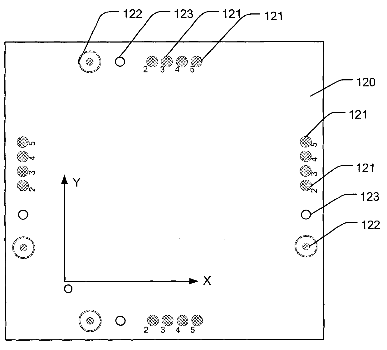
[0031] see figure 2 and image 3 , The printed circuit board provided by the present invention includes two outer layer boards 110 and at least two inner layer boards 120 . The inner board 120 is arranged between the two outer boards 110 and has specific circuits of the printed circuit board on it.

[0032] In this embodiment, the printed circuit board is a rectangular board, which includes four inner boards 120 . A test point 121 is provided on each side o...


PUM


Abstract

The invention discloses a method for measuring expansion and shrinkage of a printed circuit board, and the printed circuit board. The printed circuit board comprises two outer layer boards and at least two inner layer boards arranged between the two outer layer boards, wherein each side of each inner layer board is provided with a test point, and test points on opposite sides of each inner layer board are positioned in the same horizontal line or vertical line. Each side of each inner layer board is provided with the test point, the test points on the opposite sides of each inner layer board are positioned in the same horizontal line or vertical line, after the inner layer boards are pressed, whether the two test points of two opposite sides of each inner layer board are expanded or shrunk is measured, the expansion and shrinkage data can be accurately measured, and data support is provided for the subsequent adjustment or modification of inner layer film compensation; therefore, the adverse effect of the circuit board caused by expansion and shrinkage can be effectively improved and the rejection rate of the circuit board is reduced.

Description

technical field [0001] The invention relates to circuit board manufacturing technology, in particular to a method for measuring the expansion and contraction of a printed circuit board and the printed circuit board. Background technique [0002] Printed circuit boards are generally made of multiple boards pressed together. The outermost two-layer boards generally play the role of insulation and protection. The middle multi-layer board is an inner layer board, on which the specific circuit of the circuit board is arranged. When producing circuit boards, multiple inner boards are first pressed into one board by pressing equipment, and then pressed with two outer boards. However, when the inner boards are pressed together, one or more layers of the inner boards will expand and shrink, resulting in defective or even scrapped circuit boards. [0003] see figure 1 , the existing technology generally adopts a circular test point at the corresponding position of the four corners o...

Claims


Application Information

Patent Timeline
Patent Type & Authority Applications(China)
IPC IPC(8): G01B21/02H05K1/02
Inventor 宋国营
Owner APCB ELECTRONICS SHENZHEN CO LTD
Why Eureka
Try Eureka