

High-end PCB metallization groove processing method
A technology of metallization grooves and processing methods, applied in electrical components, printed circuit manufacturing, printed circuits and other directions, can solve problems such as affecting function and appearance, promoting conductive function, metal ring removal, etc. boosted effect
- Summary
- Abstract
- Description
- Claims
- Application Information
AI Technical Summary
Problems solved by technology
Method used
Image

Examples
Embodiment 1
[0017] A high-end PCB metallization groove processing method is characterized in that it includes the following steps: material cutting → drilling 1 → sinking copper → board electrical → outer circuit → drawing electrical → drilling 2 → etching → solder mask → text → chemical Gold→Forming→FQC→FQA→Packaging.
[0018] Further, the diameter of the drill tip used in the second drilling hole is consistent with that of the forming milling cutter.
[0019] Further, in the second drilling process, the diameters of the drill bit and the forming milling cutter used are both 2.2 mm.
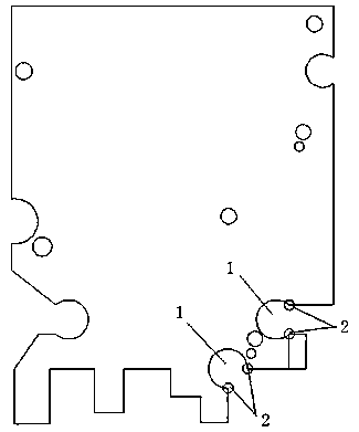
[0020] Further, during the second drilling process, the drilling position is to drill a hole 2 at both ends of the special-shaped hole 1 .
[0021] Furthermore, after the second drilling process, the copper skin ridges produced when the drill bit cuts the metal hole wall are etched to clean the excess ridges.
[0022] Further, during the forming process, the milling cutter does not directly contact the me...
Embodiment 2
[0026] A high-end PCB metallization groove processing method is characterized in that it includes the following steps: material cutting → drilling 1 → sinking copper → board electrical → outer circuit → drawing electrical → drilling 2 → etching → solder mask → text → chemical Gold→Forming→FQC→FQA→Packaging.
[0027] Further, the diameter of the drill tip used in the second drilling hole is consistent with that of the forming milling cutter.
[0028] Further, in the second drilling process, the diameters of the drill bit and the forming milling cutter used are both 1.4 mm.
[0029] Further, during the second drilling process, the drilling position is to drill a hole at both ends of the special-shaped hole.
[0030] Furthermore, after the second drilling process, the copper skin ridges produced when the drill bit cuts the metal hole wall are etched to clean the excess ridges.
[0031] Further, during the forming process, the milling cutter does not directly contact the metal o...
Embodiment 3
[0035] A high-end PCB metallization groove processing method is characterized in that it includes the following steps: material cutting → drilling 1 → sinking copper → board electrical → outer circuit → drawing electrical → drilling 2 → etching → solder mask → text → chemical Gold→Forming→FQC→FQA→Packaging.
[0036] Further, the diameter of the drill tip used in the second drilling hole is consistent with that of the forming milling cutter.
[0037] Further, in the second drilling process, the diameters of the drill bit and the forming milling cutter used are both 1.6 mm.
[0038] Further, during the second drilling process, the drilling position is to drill a hole at both ends of the special-shaped hole.
[0039] Furthermore, after the second drilling process, the copper skin ridges produced when the drill bit cuts the metal hole wall are etched to clean the excess ridges.
[0040] Further, during the forming process, the milling cutter does not directly contact the metal o...
PUM
 Abstract
Description
Claims
Application Information