Grating coupler and package structure thereof

A technology of a grating coupler and a packaging structure, applied in the field of optical communication, can solve the problems of inability to realize automatic and efficient alignment of optical fibers and gratings, incompatibility of the CMOS preparation process, and inability to carry out large-scale mass production, etc. Low, easy encapsulation, improved feasibility

Active Publication Date: 2010-12-15
TSINGHUA UNIV +1
View PDF7 Cites 23 Cited by
  • Summary
  • Abstract
  • Description
  • Claims
  • Application Information

AI Technical Summary

Problems solved by technology

Since the reflective layer is arranged between the waveguide layer and the lower cladding layer, the preparation process is incompatible with the traditional CMOS preparation process and the cost is high, so large-scale batch production cannot be carried out
[0004] In addition, how to realize the automatic alignment packaging of optical fiber and grating coupler is also a problem that must be considered in practical applications. So far, only a few packaging solutions have been initially reported in the conference report, but there is a problem in these solutions: that is, it is impossible to realize the optical fiber alignment. Automatic and efficient alignment with grating, packaging is difficult

Method used


Image

  • Grating coupler and package structure thereof
  • Grating coupler and package structure thereof
  • Grating coupler and package structure thereof

Examples


Embodiment Construction

[0032] The grating coupler of the present invention will be further described in detail below with reference to the accompanying drawings.

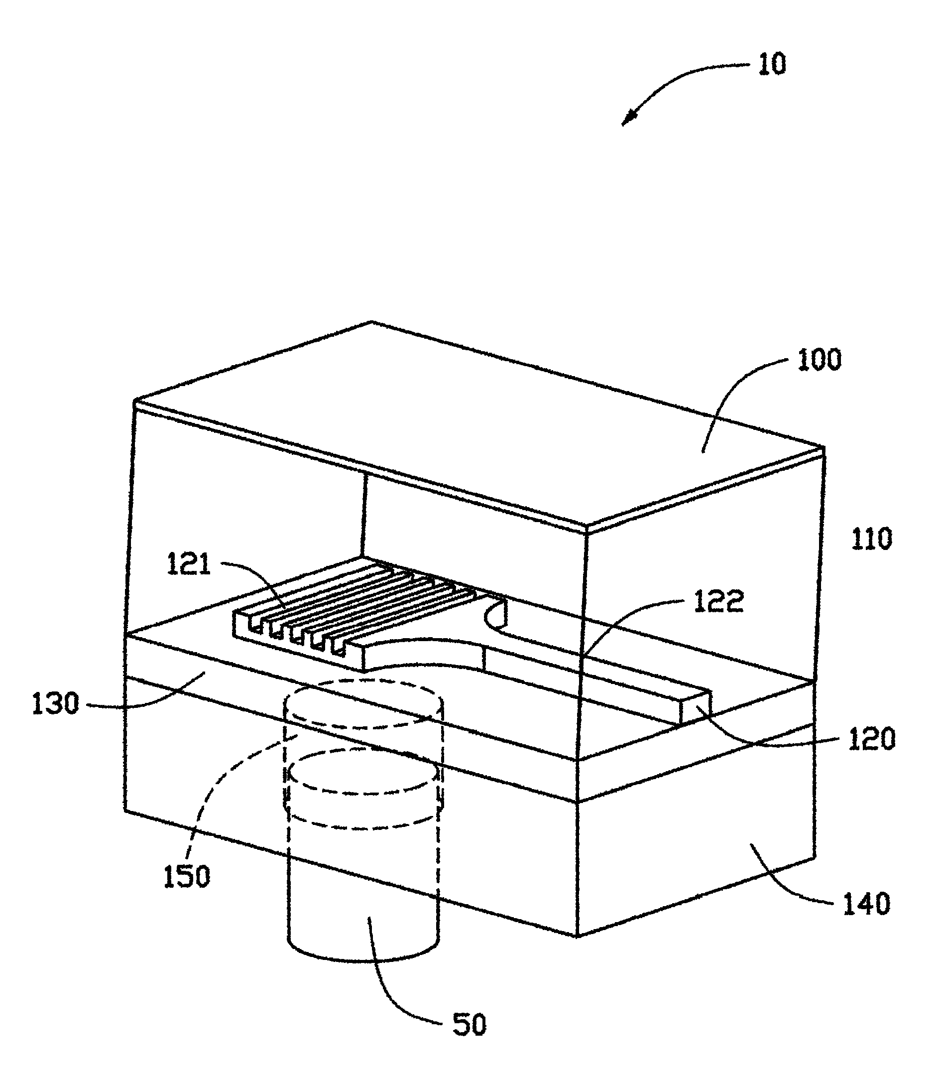
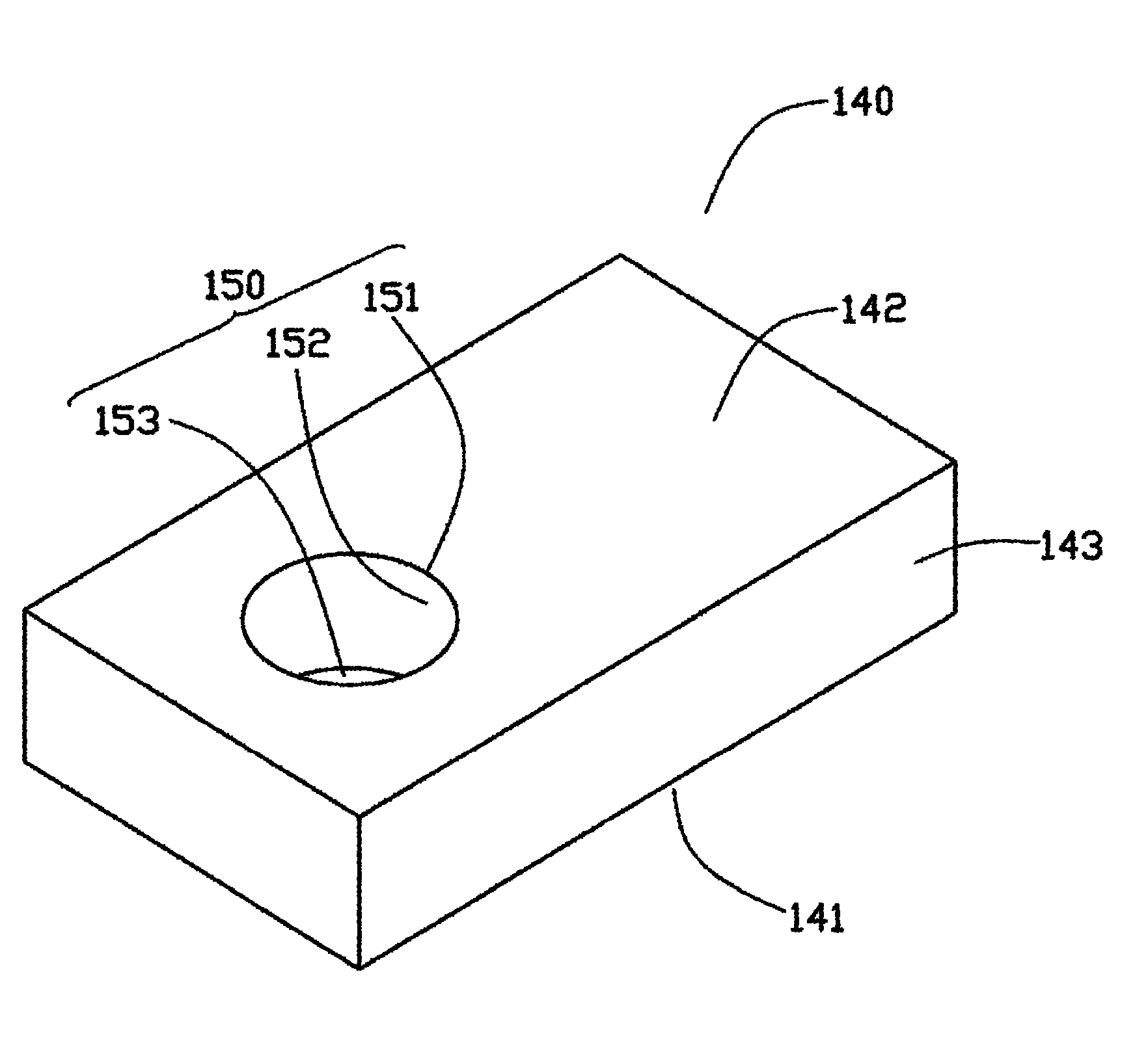
[0033] see figure 1 and figure 2 , the grating coupler 10 according to the first embodiment of the present invention includes a reflective layer 100 , an isolation layer 110 , a waveguide layer 120 , a lower cladding layer 130 and a substrate layer 140 . The substrate layer 140 has a first surface 141, a second surface 142 opposite to the first surface 141 and at least one third surface 143 connected to the first surface 141 and / or the second surface, assuming that the first surface 141 is called the front side, then the second surface 142 can be called the back side. The lower cladding layer 130 , the waveguide layer 120 , the isolation layer 110 , and the reflective layer 100 are sequentially stacked on the first surface 141 of the substrate layer 140 , and the reflective layer 100 is disposed on the surface of the isolation layer 11...


PUM


Abstract

The invention discloses a grating coupler which is high in performance, low in cost and easy to package, comprising a reflecting layer, an isolating layer, a waveguide layer, a lower cladding and a substrate layer, wherein the lower cladding layer, the waveguide layer, the isolating layer and the reflecting layer are arranged on the substrate layer in sequence; the waveguide layer is provided with a grating; and the substrate layer is provided with a fiber alignment groove. A package structure of the grating coupler provides an efficient package scheme for nano waveguide devices, reduces the process difficulty and improves the feasibility of scale package integration.

Description

technical field [0001] The invention relates to the field of optical communication, in particular to an easily packaged waveguide grating coupler. Background technique [0002] As a strong competitor of next-generation interconnection technology, optical interconnection has the characteristics of wide frequency bandwidth, anti-electromagnetic interference, strong confidentiality, low transmission loss, and low power consumption, which are obviously superior to electrical interconnection. Alternative or complementary solutions for potential electrical interconnections. With the development of semiconductor lasers, optical detectors and planar dielectric waveguide technology, as well as the micro-processing technology is becoming more and more perfect driven by the vigorous development of microelectronics technology, the realization of optoelectronic integration becomes possible. Due to the advantages of integrated optoelectronic devices such as small size, low power consumpt...

Claims


Application Information

Patent Timeline
Patent Type & Authority Applications(China)
IPC IPC(8): G02B6/34
CPCG02B6/3652G02B6/124G02B6/3644G02B6/30G02B6/34
Inventor 冯俊波李群庆范守善
Owner TSINGHUA UNIV
Why Eureka
Try Eureka