Pixel array structure

A technology of pixel array and pixel structure, applied in nonlinear optics, instruments, optics, etc., can solve the problem of inconsistent brightness of pixel structure 130

Inactive Publication Date: 2012-11-28
华映视讯(吴江)有限公司 +1
View PDF0 Cites 0 Cited by
  • Summary
  • Abstract
  • Description
  • Claims
  • Application Information

AI Technical Summary

Problems solved by technology

However, when the pixel structures 130 on different data lines 120 are interfered by signals of different polarities, the pixel structures 130 that should originally exhibit the same display brightness will have inconsistent brightness.

Method used


Image

  • Pixel array structure
  • Pixel array structure
  • Pixel array structure

Examples


Embodiment Construction

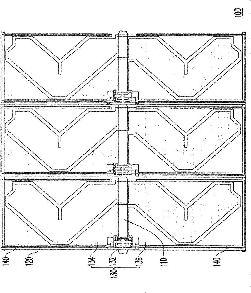
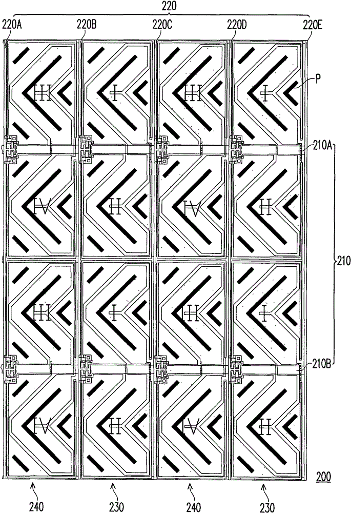
[0027] Figure 2A Shown is a pixel array structure according to an embodiment of the present invention. Please refer to Figure 2A The pixel array structure 200 includes a plurality of scan lines 210 , a plurality of data lines 220 , a plurality of first pixel structures 230 and a plurality of second pixel structures 240 . The scan line 210 intersects the data line 220 . The first pixel structures 230 and the second pixel structures 240 are alternately arranged. In fact, in this embodiment, the first pixel structures 230 and the second pixel structures 240 are arranged alternately along the extending direction of the scanning lines 210 .

[0028] For example, the pixel array structure 200 of this embodiment is, for example, applied to a liquid crystal display with stripe-type color distribution. At this time, the second pixel structures 240 electrically connected to the data line 220A and the first pixel structures 230 electrically connected to the data line 220D preferabl...


PUM


Abstract

A pixel array structure comprises a plurality of scanning lines, a plurality of data lines, a plurality of first pixel structures and a plurality of second pixel structures, wherein the scanning lines and the data lines are crossed; the first pixel structure and the second pixel structure are arranged in a staggered mode; the first pixel structure comprises a firs switching assembly, a first pixel electrode and a second pixel electrode, the first pixel electrode and the second pixel electrode are electrically connected with the first switching assembly; the second pixel structure comprises a second switching assembly, a third pixel electrode and a forth pixel electrode, the third pixel electrode and the forth pixel electrode are electrically connected with the second switching assembly; the first switching assembly and the second switching assembly are electrically connected with corresponding scanning lines and data lines; the pattern of the first pixel electrode and the pattern of the fourth pixel electrode are symmetrical about the extension direction of the scanning lines; and the pattern of the second pixel electrode and the pattern of the third pixel electrode are symmetrical about the extension direction of the scanning lines.

Description

technical field [0001] The present invention relates to a pixel array structure, and in particular to a pixel array structure formed by interlacing different pixel structures. Background technique [0002] With increasing attention to displays, many types of thin film transistor liquid crystal displays have been developed in the market, and all types of thin film transistor liquid crystal displays are developing toward higher display quality. For example, in order to reduce the display color shift of a multi-domain vertical alignment liquid crystal display, a design of dividing the pixel structure into two sub-pixel regions exhibiting different display voltages is proposed. [0003] figure 1 It is a known pixel array structure. Please refer to figure 1 , The pixel array structure 100 includes a plurality of scan lines 110 , a plurality of data lines 120 , and a plurality of pixel structures 130 . The scan lines 110 intersect with the data lines 120 , and each pixel struc...

Claims


Application Information

Patent Timeline
Patent Type & Authority Patents(China)
IPC IPC(8): G02F1/1362
Inventor 黄贵伟何建国
Owner 华映视讯(吴江)有限公司
Why Eureka
Try Eureka