
Luminous element and manufacturing method thereof

A technology for light-emitting elements and manufacturing methods, which is applied to electrical elements, electric solid-state devices, semiconductor devices, etc., and can solve the problems of poor reverse voltage value of epitaxial films, high reverse bias voltage, collapse failure, etc.

Active Publication Date: 2010-12-29
EPISTAR CORP
View PDF0 Cites 2 Cited by
  • Summary
  • Abstract
  • Description
  • Claims
  • Application Information

AI Technical Summary

Problems solved by technology

[0003] Generally, the reverse voltage value of gallium nitride series light-emitting diodes is usually around negative 15-20 volts. The main reason for the poor reverse voltage value is that the epitaxial film itself has many defects, such as lattice dislocation (dislocation), impurities (Impurity) etc. cause many leakage paths (leakage path), and the components cannot withstand high reverse bias voltage, and are prone to collapse and failure due to sudden high voltage during operation

Method used


Image

  • Luminous element and manufacturing method thereof
  • Luminous element and manufacturing method thereof
  • Luminous element and manufacturing method thereof

Examples


no. 1 example

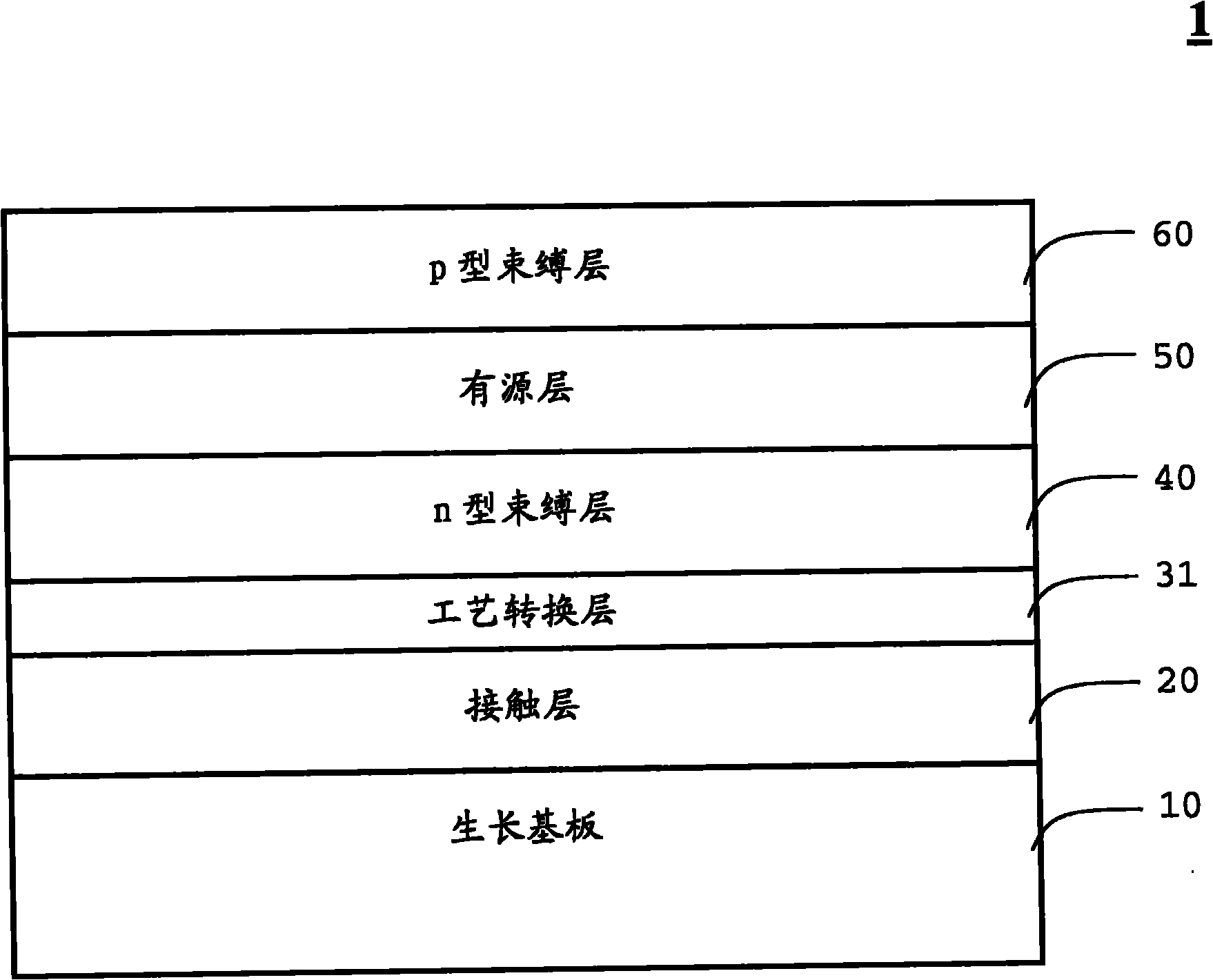
[0031] figure 1 The first embodiment of the light-emitting epitaxial structure of the light-emitting element according to the present invention is disclosed. The light-emitting epitaxial structure 1 includes a growth substrate 10, a contact layer 20 is formed on the growth substrate 10, a process conversion layer 31 is formed on the contact layer 20, and an n-type A cladding layer 40 is formed on the process conversion layer 31 , an active layer 50 is formed on the n-type cladding layer 40 , and a p-type cladding layer 60 is formed on the active layer 50 . The method for forming the light-emitting epitaxial structure 1 includes providing a growth substrate 10; then, epitaxially growing a contact layer 20 on the growth substrate 10 by metal-organic chemical vapor deposition. If the contact layer 20 has a different lattice constant from the growth substrate 10, it can be A lattice buffer layer (not shown) is grown between the contact layer 20 and the growth substrate 10 , wherei...


PUM


Abstract

The invention discloses a luminous element and a manufacturing method thereof. The luminous element has a luminous epitaxial structure. Under the condition of reverse bias voltage and the current density of -10 mA / m<2>, the absolute value of the corresponding critical reverse voltage of the luminous epitaxial structure is more than 50 V; and the luminous epitaxial structure is driven by the current density of 150mA / m<2> under the condition of forward bias voltage, the luminous element has the luminous efficiency of at least 50LM / W. The manufacturing method for the luminous element comprises the following steps of: providing a substrate; growing a first epitaxial layer on the substrate under the first growth condition; growing a process conversion layer on the first epitaxial layer under the second growth condition; and growing a second epitaxial layer on the process conversion layer under the third growth condition, wherein the first and third growth conditions have process change; and the electric conductivity of the process conversion layer is larger than that of the first epitaxial layer and / or the second epitaxial layer.

Description

technical field [0001] The present invention relates to a light-emitting element with a high critical reverse voltage and a manufacturing method thereof. Background technique [0002] Light-emitting diodes have both rectification and light-emitting effects due to their component characteristics. When a forward bias is applied to a light-emitting diode, the current value of the light-emitting diode increases rapidly as the applied forward bias increases, and emits light of a specific wavelength. The voltage value at which the current begins to rise rapidly is called The forward voltage value of the LED (Forward Voltage; Vf); when the reverse bias voltage is applied to the LED, the applied reverse bias voltage must reach a critical value before the current value rises rapidly, and the current begins to rise rapidly The voltage value is called the reverse voltage value (Reverse Voltage; Vr) of the LED. [0003] Generally, the reverse voltage value of gallium nitride series li...

Claims


Application Information

Patent Timeline
IPC IPC(8): H01L27/15H01L33/00
Inventor 张中英黄文嘉赖昭序林天坤
Owner EPISTAR CORP
Features
  • Generate Ideas
  • Intellectual Property
  • Life Sciences
  • Materials
  • Tech Scout
  • Unparalleled Data Quality
  • Higher Quality Content
  • 60% Fewer Hallucinations
Learn More