FFS (Free Fall Sensor) type TFT-LCD (Thin Film Transistor-Liquid Crystal Display) array substrate and manufacture method thereof

A technology of an array substrate and a manufacturing method, which is applied in the field of thin film transistor liquid crystal display and its manufacturing, can solve problems such as lowering the transmittance and reducing the strength of the fringe electric field, so as to reduce power consumption, increase the overall transmittance, and increase the driving frequency Effect

Active Publication Date: 2011-01-26
BOE TECH GRP CO LTD +1
View PDF0 Cites 25 Cited by
  • Summary
  • Abstract
  • Description
  • Claims
  • Application Information

AI Technical Summary

Problems solved by technology

Although this solution improves the charging and discharging characteristics of the pixel electrode by connecting part of the pixel

Method used


Image

  • FFS (Free Fall Sensor) type TFT-LCD (Thin Film Transistor-Liquid Crystal Display) array substrate and manufacture method thereof
  • FFS (Free Fall Sensor) type TFT-LCD (Thin Film Transistor-Liquid Crystal Display) array substrate and manufacture method thereof
  • FFS (Free Fall Sensor) type TFT-LCD (Thin Film Transistor-Liquid Crystal Display) array substrate and manufacture method thereof

Examples


Embodiment Construction

[0047] The technical solutions of the present invention will be described in further detail below with reference to the accompanying drawings and embodiments.

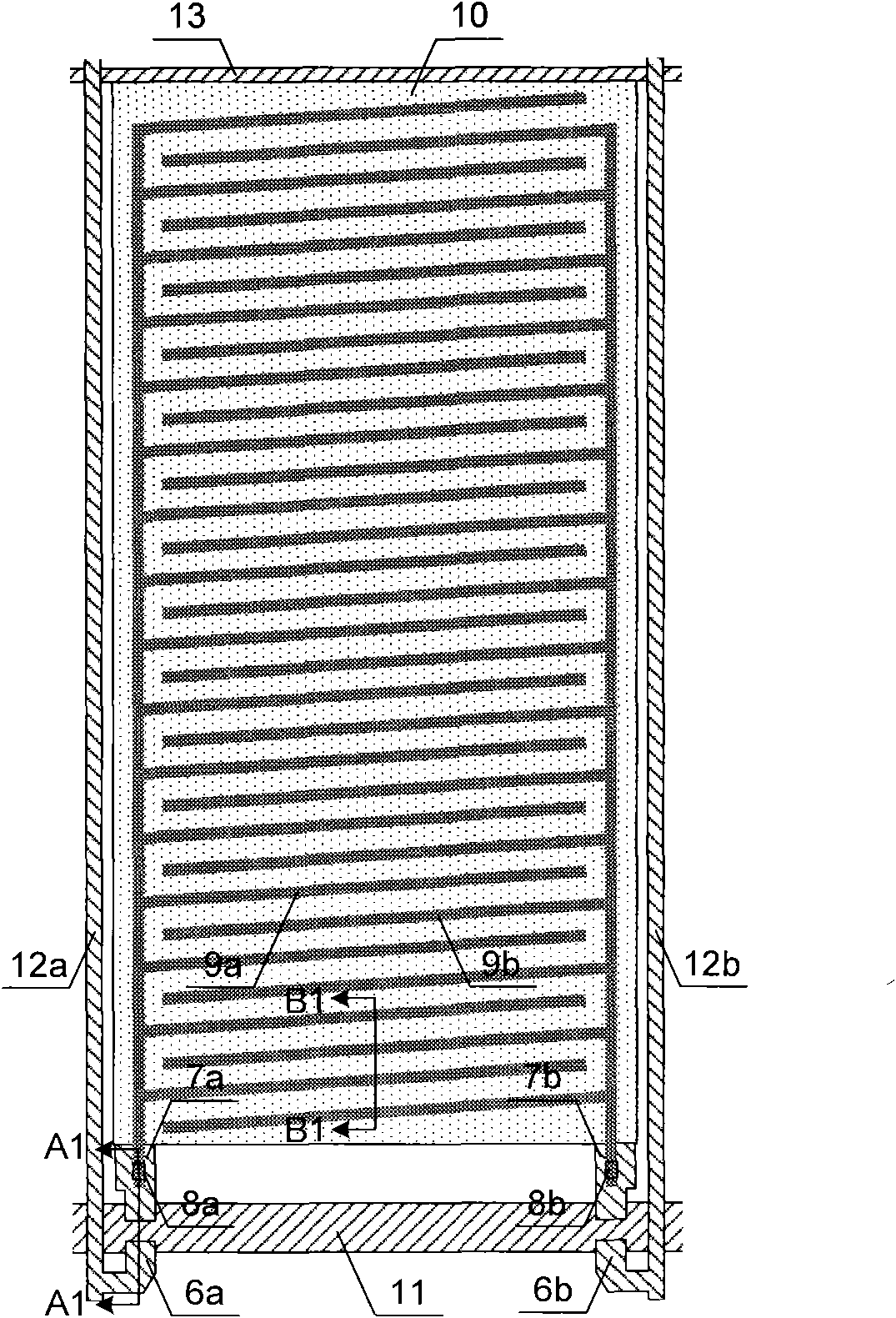
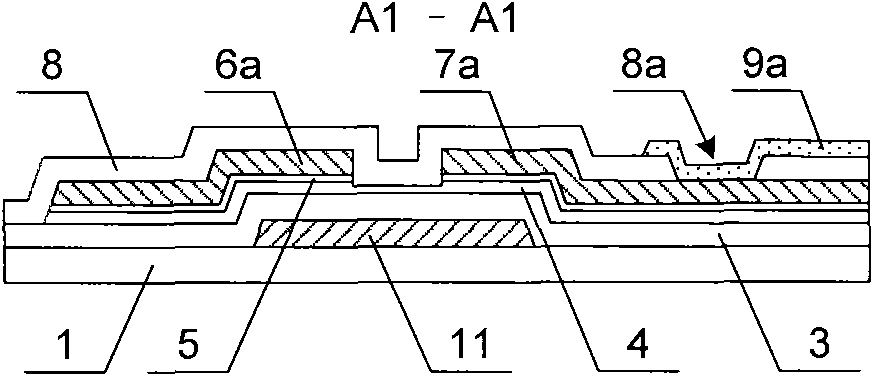
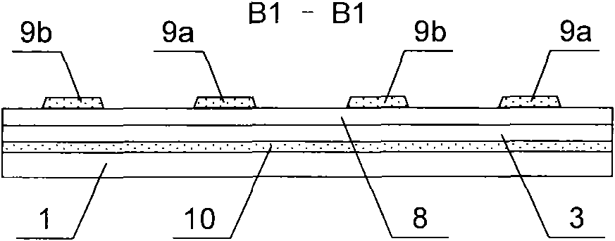
[0048] figure 1 It is a plan view of the FFS type TFT-LCD array substrate of the present invention, which reflects the structure of a pixel unit, figure 2 for figure 1 The cross-sectional view of A1-A1 in the middle, image 3 for figure 1 Sectional view of B1-B1 direction in the middle. Such as Figure 1 ~ Figure 3 As shown, the main structure of the FFS type TFT-LCD array substrate of the present invention includes a common electrode 10 formed on the substrate 1, a gate line 11, a first data line 12a, a second data line 12b, a first pixel electrode 9a, a second The pixel electrode 9b, the first thin film transistor, the second thin film transistor and the common electrode line 13; the first data line 12a and the second data line 12b arranged in parallel and two adjacent gate lines 11 define the pixel area, an...


PUM

PropertyMeasurementUnit
Widthaaaaaaaaaa

Abstract

The invention relates to an FFS (Free Fall Sensor) type TFT-LCD (Thin Film Transistor-Liquid Crystal Display) array substrate and a manufacture method thereof. The array substrate comprises a grid line, a first data line and a second data line which are formed on the substrate and limit a pixel area, wherein a common electrode, a first TFT, a second TFT, a first pixel electrode and a second pixelelectrode are formed in the pixel area; the first data line provides a first data signal to the first pixel electrode through the first TFT; the second data line provides a second data signal to the second pixel electrode through the second TFT; the first data signal and the second data signal have opposite relative polarities; and the first pixel electrode and the second pixel electrode are alternately arranged. The invention improves the equality of an electric field and has higher whole transmissivity in one aspect, improves the strength of a horizontal electric field in the other aspect, has favorable charging and discharging characteristics of the pixel electrodes, not only can improve the driving efficiency and the panel transmissivity, but also is favorable to power consumption reduction and afterimage elimination.

Description

technical field [0001] The invention relates to a thin film transistor liquid crystal display and a manufacturing method thereof, in particular to an FFS type TFT-LCD array substrate and a manufacturing method thereof. Background technique [0002] In recent years, thin film transistor liquid crystal display (Thin Film Transistor Liquid Crystal Display, TFT-LCD for short) has the characteristics of small size, low power consumption, no radiation, high display resolution, etc., and has begun to be widely popularized and become a mainstream product. Fringe Field Switching (FFS for short) is one of the technologies that have appeared in recent years that can improve the image quality of LCDs, and can simultaneously achieve the requirements of high penetration and large viewing angles. [0003] At present, the prior art FFS type TFT-LCD array substrate usually adopts the structure of single gate and single pixel electrode, including the common electrode, gate line and gate elect...

Claims


Application Information

Patent Timeline
IPC IPC(8): G02F1/1362G02F1/1368H01L21/82
Inventor 董学
Owner BOE TECH GRP CO LTD
Why Eureka
Try Eureka