Control and readout of electron or hole spin

A technology of holes and electrons, applied in the field of using the device, to achieve the effect of small size

Active Publication Date: 2011-02-02
NEWSOUTH INNOVATIONS PTY LTD
View PDF2 Cites 7 Cited by
  • Summary
  • Abstract
  • Description
  • Claims
  • Application Information

AI Technical Summary

Problems solved by technology

Fourth, Si-SET is immune to most of the charge-offset noise that interferes with Al-SET devices [9]

Method used


Image

  • Control and readout of electron or hole spin
  • Control and readout of electron or hole spin
  • Control and readout of electron or hole spin

Examples


Embodiment Construction

[0065] see now Figure 4 (a), Figure 4 (a) shows the complete device 60 for controlling and reading out the electron or hole spin of a single impurity; remember that qubits can be implemented in the electron or hole spin of a single impurity atom in silicon. Various techniques can be used to insert a single donor, for example, the techniques described in US Patent No. 7,176,066 and US Patent No. 7,061,008 can be applied.

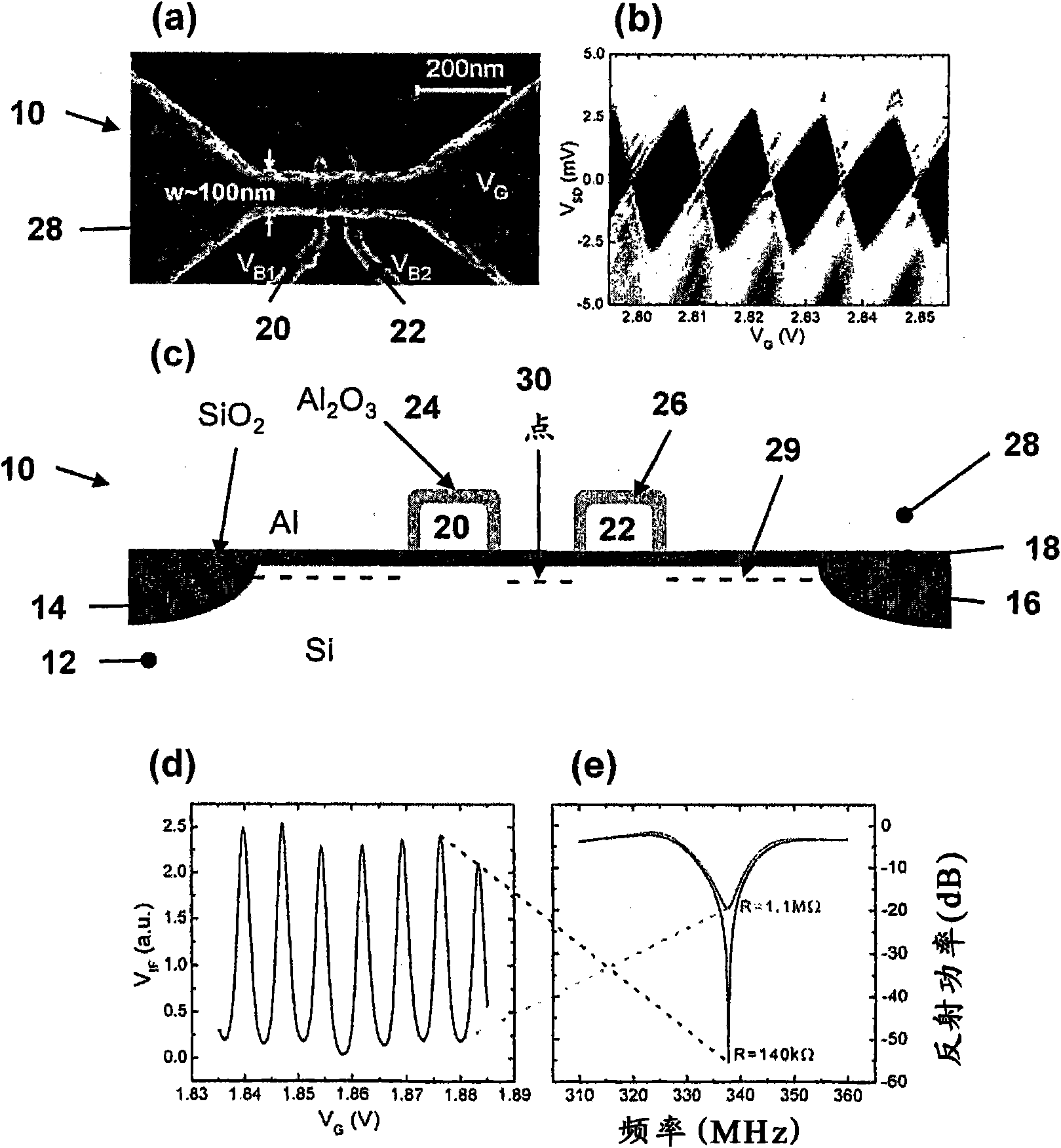
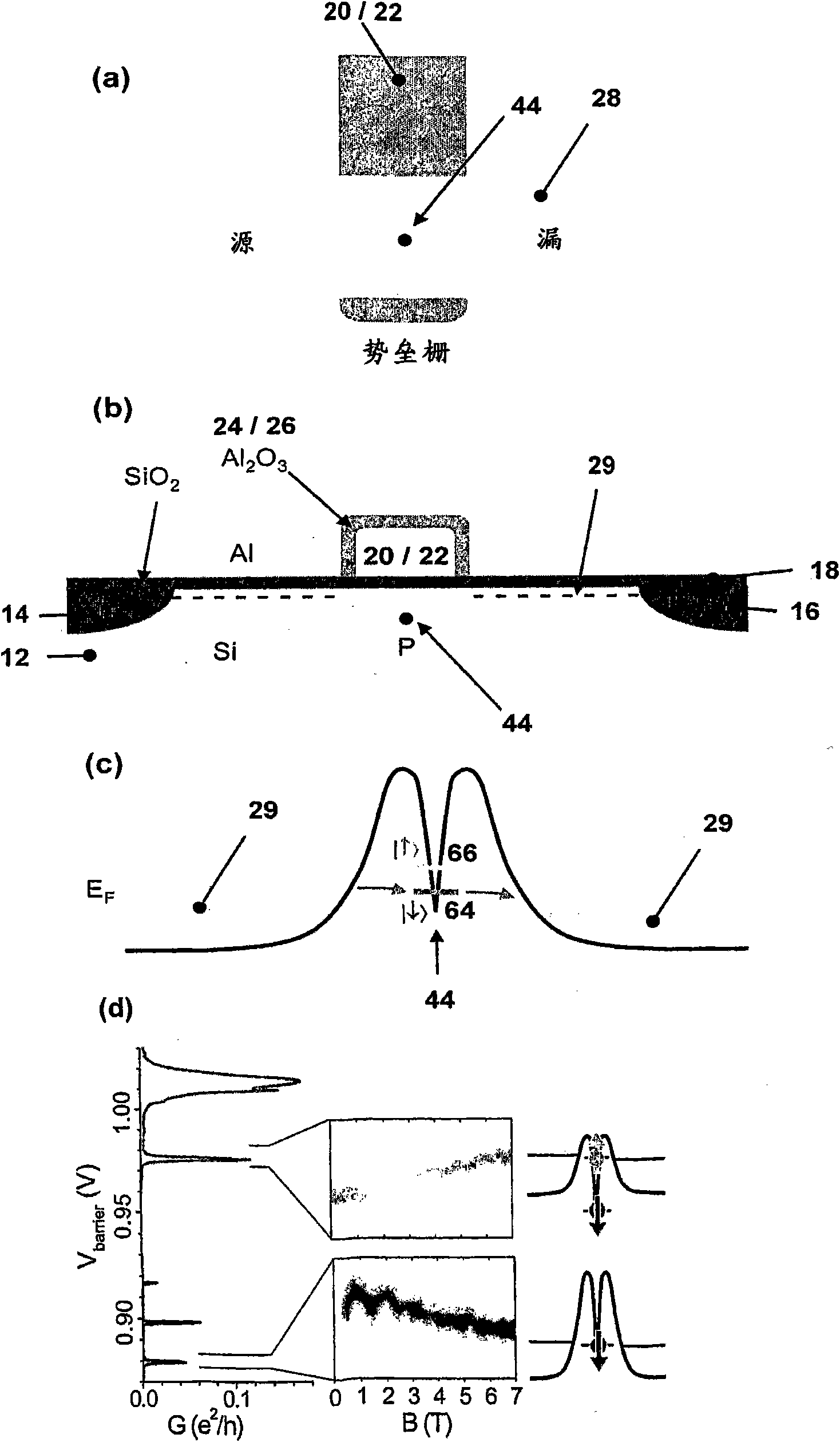
[0066] The device includes a Si-SET as shown in Fig. 1(a) and Fig. 1(c) for single-shot detection of charge transfer between impurity and pool placed separately. In this case, the impurity sites 44 are located in front of the Si-SET islands. Likewise, top gate 28 has an extended island 62 protruding toward impurity site 44 . As a result, the GICL 30 in the SET is brought close enough to the implanted impurity 44 to allow charge tunneling between them (spin dependent). The SET island 30 itself acts, in addition to its usual role, as a reservoir for spin-de...


PUM


Abstract

This invention concerns an electronic device for the control and readout of the electron or hole spin of a single dopant in silicon. The device comprises a silicon substrate in which there are one or more ohmic contact regions. An insulating region on top of the substrate. First and second barrier gates spaced apart to isolate a small region of charges to form an island of a Single Electron Transistor (SET). A third gate overlying both the first and second barrier gates, but insulated from them, the third gate being able to generate a gate-induced charge layer (GICL) in the substrate beneath it. A fourth gate in close proximity to a single dopant atom, the dopant atom being encapsulated in the substrate outside the region of the GICL but close enough to allow spin-dependent charge tunnelling between the dopant atom and the SET island under the control of gate potentials, mainly the fourth gate. In use either the third or fourth gate also serve as an Electron Spin Resonance (ESR) line to control the spin of the single electron or hole of the dopant atom. In a further aspect it concerns a method for using the device.

Description

technical field [0001] The invention relates to an electronic device for controlling and reading out the electron or hole spin of a single impurity in silicon. In another aspect, the invention relates to a method of using the device. Background technique [0002] Several important milestones have been achieved on the road to building scalable silicon-based quantum computers. Most important are: the development of single ion implantation techniques that allow the precise placement of individual phosphorus atoms in silicon [1]; the application of advanced nanofabrication, microwave, and cryogenic techniques to single-electron transistors with charge sensitivity approaching the quantum limit (rf-SET) production and characterization [2]; control and detection of single electron migration between individual phosphorus donors obtained by combining single ion implantation and SET technology [3]; and for general fault-tolerant quantum Calculation and subsequent analysis of the err...

Claims


Application Information

Patent Timeline
Patent Type & Authority Applications(China)
IPC IPC(8): G06N99/00G01N24/10H01L21/335H01L21/8238
CPCB82Y10/00H01L29/7613G01N24/10G06N99/002H01L29/66984G06N10/00
Inventor 安德里亚·莫雷洛安德鲁·史蒂夫·德祖瑞克汉斯-格列戈尔·许布尔罗伯特·格雷厄姆·克拉克劳伦斯·亨利·威廉斯·范·贝韦雷恩洛伊德·克里斯托弗·伦纳德·霍伦贝格大卫·诺曼·贾米森克里索弗·埃斯科特
Owner NEWSOUTH INNOVATIONS PTY LTD
Why Eureka
Try Eureka