Low-voltage high-gain high-speed germanium photo detector and method of fabricating the same

a germanium photo detector and high-gain technology, applied in the field of photodetectors, can solve the problems of high operation voltage for achieving high sensitivity, high fabrication cost, high power consumption, etc., and achieve the effects of high gain, low voltage and high speed

Active Publication Date: 2014-02-20
ELECTRONICS & TELECOMM RES INST
View PDF4 Cites 21 Cited by
  • Summary
  • Abstract
  • Description
  • Claims
  • Application Information

AI Technical Summary

Problems solved by technology

Especially, a CMOS-compatible cost-effective high-performance germanium photo detector is being actively researched to realize an ultra-high-speed large capacity optical communication system and an image processing system, and speed and sensitivity of the photo detector are emerging as major issues.
The III-V compound semiconductor-based avalanche optical receiver suffers from high fabrication cost and a high operation voltage for achieving high sensitivity.
Nevertheless, to achieve high gain and high sensitivity, the silicon-based avalanche photodetector should be operated at a very high operation voltage (e.g., an avalanche voltage), and thus, it suffers from high power consumption.

Method used


Image

  • Low-voltage high-gain high-speed germanium photo detector and method of fabricating the same
  • Low-voltage high-gain high-speed germanium photo detector and method of fabricating the same
  • Low-voltage high-gain high-speed germanium photo detector and method of fabricating the same

Examples


first embodiment

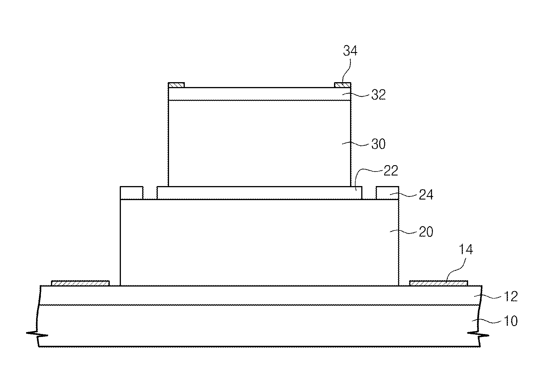
[0047]FIG. 1 is a sectional view illustrating a photodetector according to the inventive concept.

[0048]Referring to FIG. 1, the photodetector according to the first embodiment of the inventive concept may include a substrate 10, a first contact layer 12, a first electrode 14, a carrier multiplication layer 20, a charge layer 22, an absorption layer 30, a second contact layer 32, and a second electrode 34.

[0049]The substrate 10 may include silicon. The first contact layer 12 may include silicon doped with first impurities. The first impurities may be n-type donors, such as phosphorous. For example, the first contact layer 12 may include n++ silicon. The carrier multiplication layer 20 and the first electrode 14 may be provided on the first contact layer 12.

[0050]The carrier multiplication layer 20 may include intrinsic germanium. The carrier multiplication layer 20 may be configured to amplify an electrical signal in the absorption layer 30. For example, the carrier multiplication la...

second embodiment

[0061]FIG. 6 is a sectional view illustrating a photodetector according to the inventive concept.

[0062]Referring to FIG. 6, the photodetector according to the second embodiment of the inventive concept may include a super lattice structure consisting of a third material layer 31 and a fourth material layer 33, which may be provided as the absorption layer 30. The second embodiment may differ from the first embodiment, in that intrinsic germanium of the absorption layer 30 is replaced with the superlattice structure. The third and fourth material layers 31 and 33 of the superlattice structure may be different from each other in terms of a mixing ratio (mole fraction) of silicon to germanium. For example, the third material layer 31 may include Si1-xGex, and the fourth material layer 33 may include Si1-yGey.

[0063]FIG. 7 is a sectional view illustrating a photodetector according to a third applied embodiment of the inventive concept.

[0064]Referring to FIG. 7, the photodetector accordin...

third embodiment

[0066]FIG. 8 is a sectional view illustrating a photodetector according to the inventive concept.

[0067]Referring to FIG. 8, the photodetector according to the third embodiment of the inventive concept may include the absorption layer 30 including both of a superlattice layer 36 and an intrinsic layer 38. According to the third embodiment, the absorption layer 30 of the first embodiment may be replaced with the superlattice layer 36 and the intrinsic layer 38. As shown in FIG. 8, the superlattice layer 36 and the intrinsic layer 38 may be formed to have the same thickness (e.g., half the thickness of the absorption layer 30) as each other, but example embodiments of the inventive concept may not be limited thereto. The superlattice layer 36 may be a silicon / germanium superlattice and include the third material layer 31 and the fourth material layer 33. The third material layer 31 may include Si1-xGex, and the fourth material layer 33 may include Si1-yGey. The intrinsic layer 38 may i...


PUM


Abstract

Provided is a silicon-wafer-based germanium semiconductor photodetector configured to be able to provide properties of high gain, high sensitivity, and high speed, at a relatively low voltage. A germanium-based carrier multiplication layer (e.g., a single germanium layer or a germanium and silicon superlattice layer) may be provided on a silicon wafer, and a germanium charge layer may be provided thereon, a germanium absorption layer may be provided on the charge layer, and a polysilicon second contact layer may be provided on the absorption layer. The absorption layer may be configured to include germanium quantum dots or wires.

Description

CROSS-REFERENCE TO RELATED APPLICATIONS[0001]This U.S. non-provisional patent application claims priority under 35 U.S.C. §119 to Korean Patent Application Nos. 10-2012-0090860, 10-2013-0033585, and 10-2013-0061169, filed on Aug. 20, 2012, Mar. 28, 2013, and May 29, 2013, respectively, in the Korean Intellectual Property Office, the entire contents of which are hereby incorporated by reference.BACKGROUND OF THE INVENTION[0002]Example embodiments of the inventive concept relate to a photodetector, and in particular, to a low-voltage high-gain high-speed germanium detector realized on a silicon substrate.[0003]Recently, silicon photonics is actively being researched. Especially, a CMOS-compatible cost-effective high-performance germanium photo detector is being actively researched to realize an ultra-high-speed large capacity optical communication system and an image processing system, and speed and sensitivity of the photo detector are emerging as major issues. Further, there is an i...

Claims


Application Information

Patent Timeline
Patent Type & Authority Applications(United States)
IPC IPC(8): H01L33/06H01L33/00
CPCH01L33/06H01L33/0054B82Y20/00Y10S977/774Y10S977/954Y10S977/762H01L31/035227H01L31/035254H01L31/107
Inventor KIM, GYUNGOCKKIM, SANG HOONJANG, KI SEOKKIM, IN GYOOOH, JIN HYUKKIM, SUN AE
Owner ELECTRONICS & TELECOMM RES INST
Why Eureka
Try Eureka