
Organic electroluminescence element

A kind of electroluminescence, electromechanical technology, applied in the direction of electrical components, electro-solid devices, circuits, etc., can solve the problems of device characteristics obstacles, and achieve the effect of improving resistance, high color reproducibility and good reproducibility

Inactive Publication Date: 2011-03-23
YAMAGATA PROMOTIONAL ORG FOR INDAL TECH
View PDF3 Cites 6 Cited by
  • Summary
  • Abstract
  • Description
  • Claims
  • Application Information

AI Technical Summary

Problems solved by technology

[0012] Therefore, the structure of the intermediate layer as described above hinders the improvement of the characteristics of the device, and it is required to improve the structure of the intermediate layer from the viewpoint of high efficiency and long life.

Method used


Image

  • Organic electroluminescence element
  • Organic electroluminescence element
  • Organic electroluminescence element

Examples


Embodiment 1

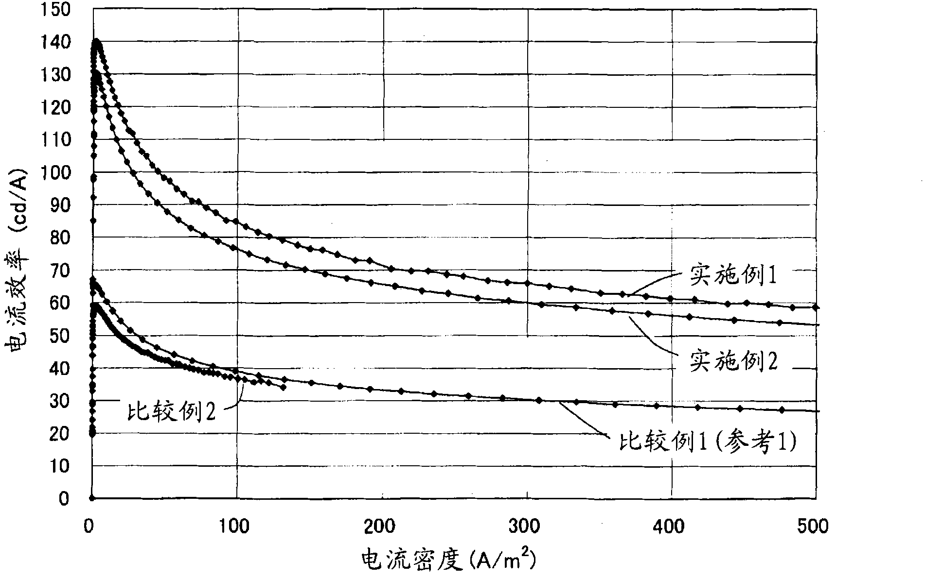
[0090] First, ultrasonic cleaning using pure water and surfactant, running water cleaning using pure water, ultrasonic cleaning using a 1:1 mixed solution of pure water and isopropanol, and boiling cleaning using isopropanol Sequentially, cleaning treatment was performed on the glass substrate on which the patterned transparent conductive film (ITO) was formed with a film thickness of 110 nm. The substrate was slowly lifted from boiling isopropanol, dried in isopropanol vapor, and finally cleaned with ultraviolet ozone.

[0091] The substrate was arranged in a vacuum chamber, and the vacuum was exhausted to 1×10 -6 Torr, each molybdenum boat (boat) filled with vapor deposition materials and a vapor deposition mask for forming a film in a predetermined pattern are set in advance in this vacuum chamber, and the boat is heated by energization to make the vapor deposition The materials were evaporated, and a hole transport layer, a first light-emitting unit, an intermediate layer...

Embodiment 2

[0102] Using the layer structure shown in Example 2 of Table 1, a green phosphorescent element with a two-stage multiphoton structure was produced in the same procedure as in Example 1.

[0103] The intermediate layer is a co-evaporated layer of spiro-DPVBi and molybdenum trioxide, and a layer of only spiro-DPVBi is formed between the spiro-TAD layer, and molybdenum trioxide and spiro-TDA which is an arylamine compound are not in direct contact.

Embodiment 3

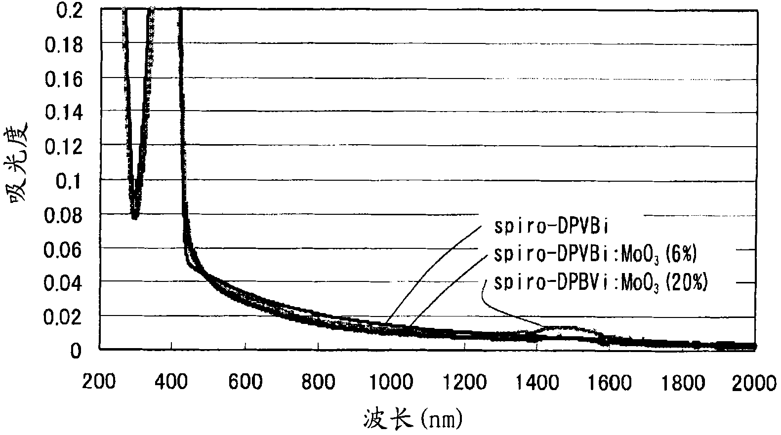
[0119] Formation of a spiro-DPVBi monomer film with a thickness of 50nm and MoO 3 Co-evaporated film, and its UV absorption spectrum was measured.

[0120] exist image 3 These UV absorption spectra are shown in .


PUM


Abstract

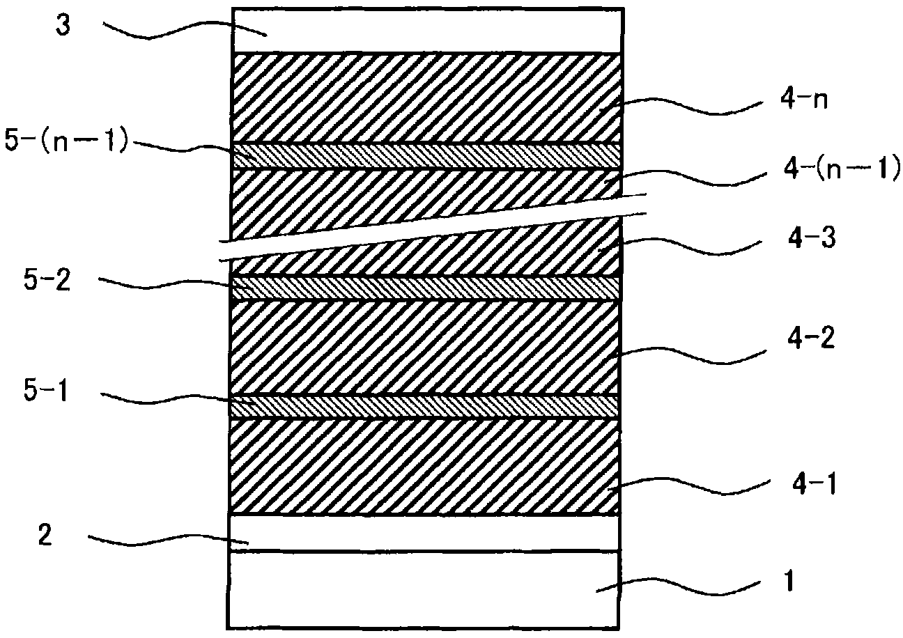
The invention relates to an organic electroluminescence element. The present invention provides an organic EL element having a multi-photon structure, in which optical absorption in the visible region caused by a charge-transfer complex in a conventional intermediate layer structure is inhibited, and the resistance of this intermediate layer to a counter career is improved, thus allowing high efficiency and a long operation life of the element. The element is arranged to be formed on a substrate 1 and have a multi-photon structure in which a plurality of light emitting units 4 including at least one light emitting layer are stacked via an intermediate layer 5 between an anode layer 2 and a cathode layer 3 which is a counter electrode, the above-mentioned intermediate layer 5 is formed by mixing or stacking an electron accepting material or an electron donating material and an organic compound, so as to avoid formation of a charge-transfer complex.

Description

technical field [0001] The present invention relates to a light-transmitting organic electroluminescent (EL) element suitable for lighting. Background technique [0002] Organic EL elements are self-luminous elements that use organic compounds as light-emitting materials. Since they can emit light at a high speed, they are suitable for displaying moving images. In addition, they have the characteristics of simplifying the structure of the element and reducing the thickness of the display panel. Because of such excellent characteristics, organic EL elements are widely used in daily life as displays for mobile phones and vehicles. [0003] In addition, in recent years, it has attracted attention as next-generation lighting by making use of the advantages of the above-mentioned thin surface emission. [0004] A multi-photon structure (multi-photon structure) has been proposed as one of methods for achieving high efficiency and long life of the organic EL element in order to im...

Claims


Application Information

Patent Timeline
Patent Type & Authority Applications(China)
IPC IPC(8): H01L51/50H01L51/52H01L51/54
CPCH01L51/5036H01L51/5278H10K50/125H10K50/19H01L2924/01042H01L2924/01074H10K85/631
Inventor 小田敦田中纯一河合崇
Owner YAMAGATA PROMOTIONAL ORG FOR INDAL TECH
Learn More