Method for forming semiconductor device

A semiconductor and device technology, applied in the field of semiconductor device formation, can solve problems such as bulging, device performance degradation, defects, etc., and achieve the effect of reducing the number of defects

Inactive Publication Date: 2011-03-30
SEMICON MFG INT (SHANGHAI) CORP +1
View PDF1 Cites 9 Cited by
  • Summary
  • Abstract
  • Description
  • Claims
  • Application Information

AI Technical Summary

Problems solved by technology

[0009] With the further development of the production scale of the integrated circuit, the metal layer material of the metal layer 14 is mainly Cu, the metal layer 14 formed will have stress, and in the subsequent process, a multilayer covering layer will be formed

Method used


Image

  • Method for forming semiconductor device
  • Method for forming semiconductor device
  • Method for forming semiconductor device

Examples


Example Embodiment

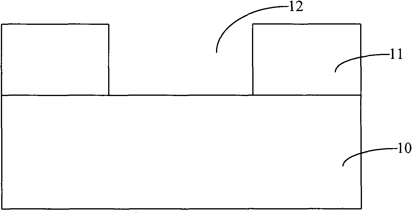
[0016] After a large number of experiments, the inventor of the present invention found that the metal layer formed on the semiconductor substrate does not match the material of the semiconductor substrate. The metal layer formed by the prior art usually has tensile stress. In the further development of the metal layer, a multi-layer film is usually formed on the surface of the metal layer, so that the stress of the metal layer is further expanded, and there will be a multi-step high temperature process after the metal layer is formed. The metal layer and the semiconductor substrate And the subsequent thermal expansion coefficients of the films formed on the surface of the metal layer are not the same. In the multi-step high temperature process, bulging and defects will occur on the surface of the metal layer, resulting in a decrease in device performance.

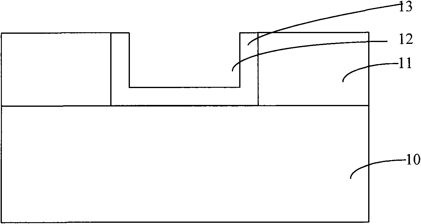
[0017] To this end, the present invention provides a method for forming a semiconductor device, Figure 5 It is a schematic ...


PUM

PropertyMeasurementUnit
Thicknessaaaaaaaaaa

Abstract

A method for forming a semiconductor device comprises the following steps: providing a substrate; forming a dielectric layer on the surface of the substrate; forming a via exposing the substrate on the dielectric layer; forming a metal layer filling the via on the surface of the dielectric layer; carrying out heat treatment on the metal layer; and forming a covering layer on the surface of the metal layer after heat treatment. The invention can avoid bulge and defects on the surface of the metal layer and improve the performance of the device.

Description

technical field [0001] The invention relates to the field of semiconductor manufacturing, in particular to a method for forming a semiconductor device. Background technique [0002] As the production of integrated circuits develops towards ultra-large-scale integrated circuits, the circuit density inside integrated circuits is increasing, and the number of components contained is also increasing. This development makes the surface of the wafer unable to provide enough area to manufacture all the components. required interconnection wires. [0003] In order to meet the requirements of interconnection lines after shrinking components, the design of two or more layers of multilayer metal interconnection lines has become a method commonly used in VLSI technology. At present, the conduction between different metal layers or the metal layer and the liner layer is to form an opening through the dielectric layer between the metal layer and the metal layer or between the metal layer...

Claims


Application Information

Patent Timeline
IPC IPC(8): H01L21/768H01L21/321
Inventor 王琪
Owner SEMICON MFG INT (SHANGHAI) CORP
Why Eureka
Try Eureka