Anti-etching layer, semiconductor processing device and manufacturing method

A processing device and manufacturing method technology, applied in coating, metal material coating process, gaseous chemical plating, etc., can solve the problem of increasing user cost, damage to MOCVD equipment chamber, and reducing the use of MOCVD equipment chamber and processing components Life and other issues, to achieve the effect of improving service life, reducing surface damage, and reducing use costs

Inactive Publication Date: 2011-11-30
ADVANCED MICRO FAB EQUIP INC CHINA
View PDF5 Cites 4 Cited by
  • Summary
  • Abstract
  • Description
  • Claims
  • Application Information

AI Technical Summary

Problems solved by technology

[0006] It has been found in practice that the plasma used in the above-mentioned in-situ chemical cleaning method will damage the inside of the MOCVD equipment chamber and the surface of the processing comp

Method used


Image

  • Anti-etching layer, semiconductor processing device and manufacturing method
  • Anti-etching layer, semiconductor processing device and manufacturing method
  • Anti-etching layer, semiconductor processing device and manufacturing method

Examples


Embodiment Construction

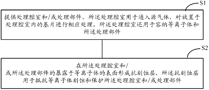
[0035] For equipment that uses plasma for process treatment, such as plasma etching equipment, plasma enhanced chemical vapor deposition equipment, MOCVD (using plasma to clean processing chambers and processing components), its processing chambers and processing components are vulnerable to plasma body etching damage, an embodiment of the present invention proposes a semiconductor processing device, including:

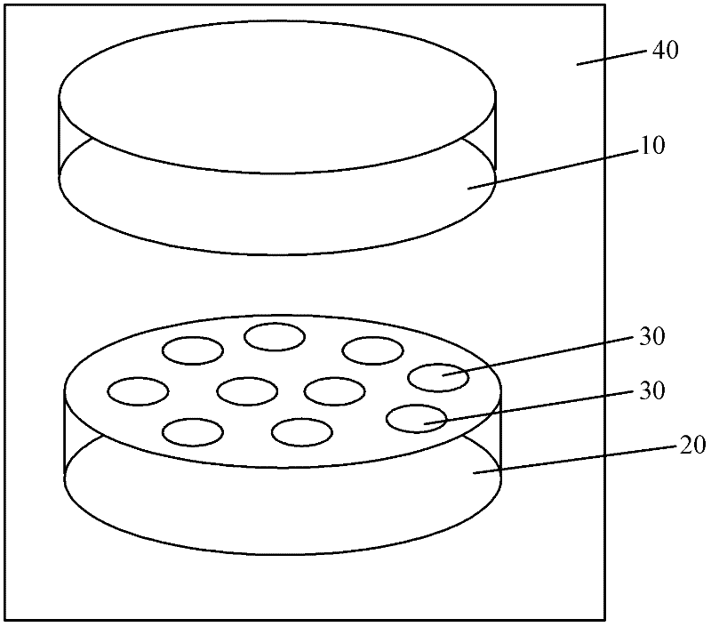
[0036] A processing chamber, the processing chamber is used to feed the source gas to perform corresponding processing on the substrate placed in the processing chamber, and the processing chamber is also used to accommodate plasma, and there are multiple processing chambers in the chamber components, the semiconductor processing apparatus further comprising:

[0037]Anti-etching layer covering the surface of the processing chamber and / or processing components exposed to plasma, the anti-etching layer is used to resist plasma etching and protect the processing chamber...


PUM


Abstract

Embodiments of this invention provide an anti-etching layer, a semiconductor processing device and its fabrication method. The semiconductor processing device comprises a processing chamber configured for the source gas introduction for corresponding to the treatment of substrates placed in the processing chamber. The processing chamber is further configured to receive the plasma and has a plurality of processing parts therein. The semiconductor processing device further comprises: an anti-etching layer covered on the surface of the processing chamber and/or processing parts exposed to the plasma. The anti-etching layer is used to resist the plasma etching and protect the processing chamber and/or processing parts. This invention uses the anti-etching layer to protect the processing chamber and processing parts to prevent them from being damaged by the plasma and increase their service lives.

Description

technical field [0001] The invention relates to the technical field of semiconductors, in particular to an anti-etching layer, a semiconductor processing device and a manufacturing method thereof. Background technique [0002] MOCVD is the English abbreviation of Metal-organic Chemical Vapor Deposition. MOCVD is a new type of vapor phase epitaxial growth technology developed on the basis of vapor phase epitaxial growth (VPE). It uses organic compounds of Group III and II elements and hydrides of Group V and VI elements as crystal growth source materials, and performs vapor phase epitaxy on the substrate in a thermal decomposition reaction mode to grow various III-V, II- Thin-layer single-crystal materials of group VI compound semiconductors and their multi-component solid solutions. Usually the crystal growth in the MOCVD system is carried out in a cold-walled quartz (stainless steel) reaction chamber at normal pressure or low pressure (10-100Torr), and H 2 As a carrier g...

Claims


Application Information

Patent Timeline
IPC IPC(8): C23C16/00C23C30/00
Inventor 贺小明倪图强杨平万磊
Owner ADVANCED MICRO FAB EQUIP INC CHINA
Why Eureka
Try Eureka