Developing device

A developing device and developing solution technology, which is applied in the processing of photosensitive materials, etc., can solve the problems of photoresist denaturation, increasing the amount of developing solution, and prone to defects, etc., and achieve the effects of reducing the number of defects, improving cleaning efficiency, and improving the effect

Inactive Publication Date: 2012-07-11
CSMC TECH FAB2 CO LTD
View PDF2 Cites 5 Cited by
  • Summary
  • Abstract
  • Description
  • Claims
  • Application Information

AI Technical Summary

Problems solved by technology

[0003] Generally, the surface of photoresist is hydrophobic, while the developer is hydrophilic. Therefore, when the developer is sprayed on the surface of the wafer, it may not be able to completely cover the entire surface of the wafer, resulting in part of the photoresist not being wetted and developed.
A common improvement method is to use the cleaning nozzle to spray deionized water on the surface of the wafer first, then rotate the wafer to shake off the deionized water, so as to retain a thin layer of water film on the surface of the wafer, so as to improve the impact of the developer on the wafer. coverage, but the actual process is difficult to control, such as: when the rotation speed of the wafer is too high, the water film cannot be retained on the surface of the wafer; while the rotation speed is too low, the water film retained on the surface of the wafer will be uneven. The method of pre-wetting with ionized water cannot completely solve the problems caused by the hydrophobicity of the photoresist and the hydrophilicity of the developer
[0004] In addition, since the photoresist is generally acidic and the developer is alkaline, when the developer is directly sprayed onto the surface of the photoresist, the pH of the photoresist surface will change sharply (PH shock), resulting in denaturation of the photoresist. cannot be removed by development
In most cases, the developer is sprayed at the center of the wafer, and then rotated at a low speed to spread out to the periphery, so the center of the wafer will always be in contact with fresh developer, resulting in excessive reaction in the center of the wafer. The common solution is In the case of high-speed rotation of the wafer, the developer is sprayed to the center of the wafer for a long time for pre-wetting, but the consequence is that the amount of developer is increased, and defects are prone to occur
[0005] The defect control of photolithography development depends largely on the final cleaning process. Since the photoresist is hydrophobic, generally increasing the cleaning time and water pressure can reduce particles and photoresist residues to effectively reduce defects, however, are also likely to result in the collapse of the lithographic pattern

Method used


Image

  • Developing device
  • Developing device

Examples


Embodiment Construction

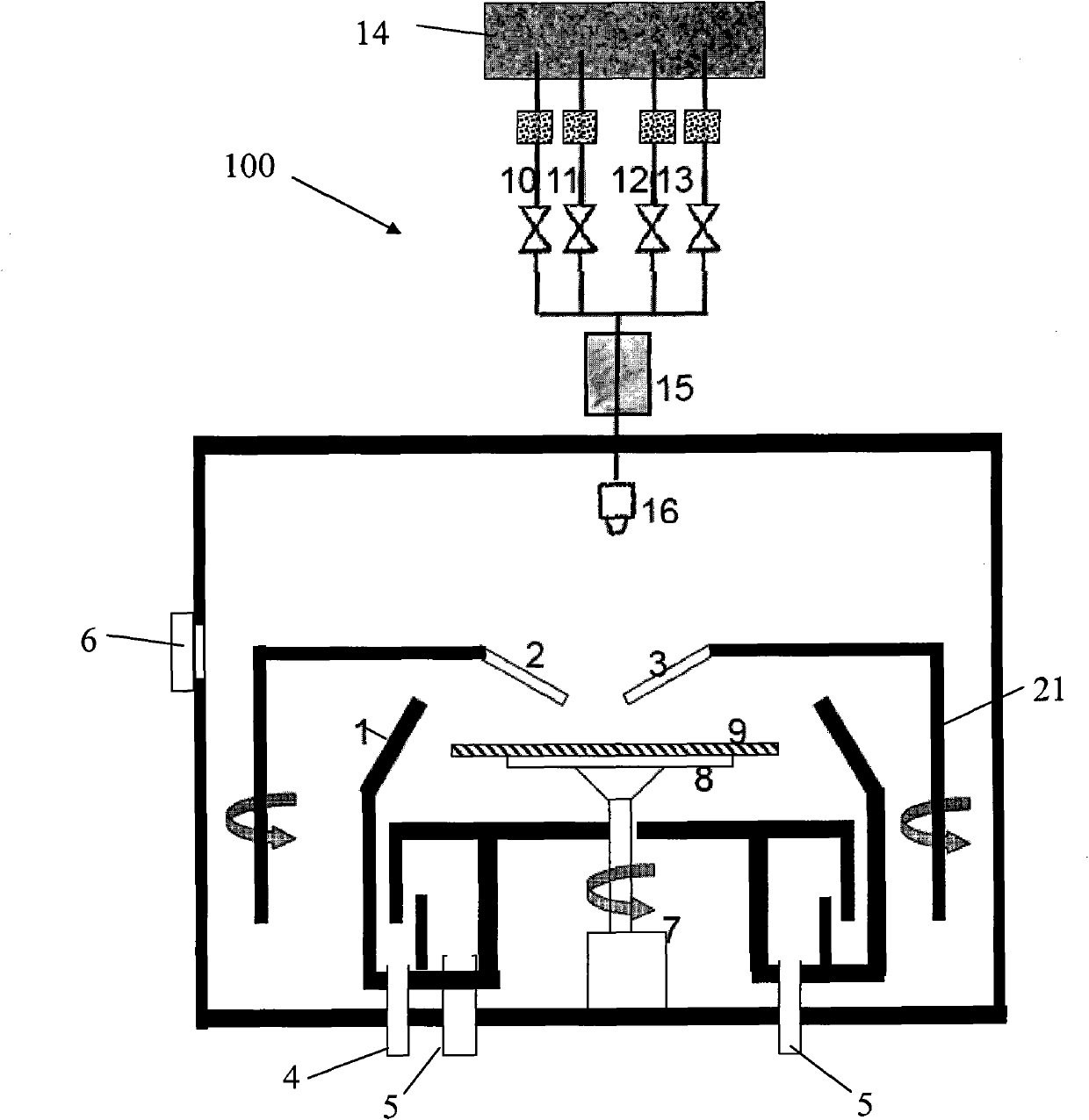
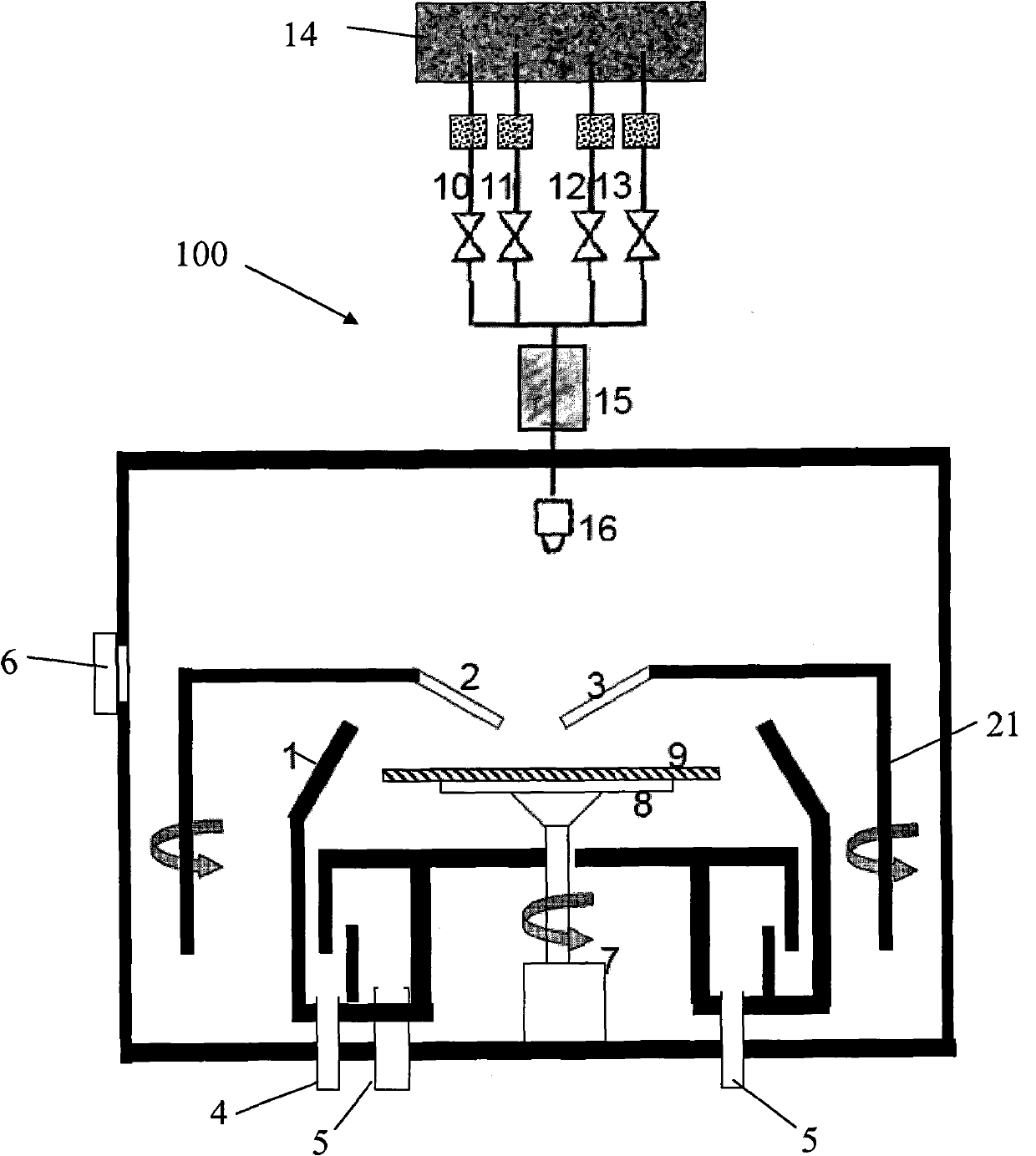
[0017] see figure 1 As shown, the present invention provides a developing device 100, which is used for photolithographic development in the semiconductor manufacturing process. The developing device 100 includes a developing chamber 1, a cleaning nozzle 2, a developing solution nozzle 3, a waste liquid discharge port 4, and a developing chamber exhaust. The control terminal 5 , the wafer 9 conveying the control port 6 , the motor 7 , the vacuum chuck 8 , the control module 14 , the atomizing device 15 and the mist nozzle 16 . In the photolithography development process described in the present invention, the development device 100 needs to use deionized water, a surfactant solution, an organic alcohol mixed solution mixed with an organic solvent such as ethanol, and a developer to process the wafer 9. Wetting, cleaning, and removing the photoresist on the wafer 9 to form the required circuit patterns on the wafer.

[0018] All main working components of the developing device...


PUM


Abstract

The invention provides a developing device, which comprises a developing cavity, a tray which is arranged in the developing cavity and used for holding a wafer, and a cleaning nozzle and a developing liquid nozzle which are positioned above the tray and can be adjusted, a control module, an atomizing device and an atomized liquid nozzle positioned above the tray, wherein the atomizing device and the atomized liquid nozzle are controlled by the control module; and a temperature control unit is arranged in the atomizing device. Compared with the prior art, the developing device is provided with the atomizing device and the atomized liquid nozzle, so that atomized liquid sprayed by the atomized liquid nozzle can cover the whole wafer once, so that an effect of pre-infiltrating the wafer is improved remarkably, the cleaning efficiency is improved, and the number of defects is reduced.

Description

【Technical field】 [0001] The invention relates to a developing device, in particular to a developing device applied in the photolithography process of semiconductor integrated circuits. 【Background technique】 [0002] Developing is a basic process in the photolithography process of semiconductor integrated circuits. It is to use a weak alkaline solution to remove the unnecessary photoresist after exposure on the wafer, leaving only the required strips, holes and other circuits on the wafer. graphics. The line width resolution formed after development, the line width uniformity of graphics, particles and defects, development cost and time, etc. are important factors for evaluating the development process. [0003] The surface of the general photoresist is hydrophobic, but the developer is hydrophilic. Therefore, when the developer is sprayed on the surface of the wafer, it may not be able to completely cover the entire surface of the wafer, resulting in part of the photoresi...

Claims


Application Information

Patent Timeline
Patent Type & Authority Applications(China)
IPC IPC(8): G03F7/30
Inventor 黄玮
Owner CSMC TECH FAB2 CO LTD
Why Eureka
Try Eureka