Reference voltage compensating device and method

A technology of reference voltage and voltage compensation, which is applied in the direction of instruments and static indicators, etc., can solve the problems of poor quality, uneven distribution of common electrode voltage, residual image quality of display screen images, etc., and achieve the effect of improving image quality and reducing image retention

Active Publication Date: 2011-04-06
BEIJING BOE OPTOELECTRONCIS TECH CO LTD
View PDF0 Cites 33 Cited by
  • Summary
  • Abstract
  • Description
  • Claims
  • Application Information

AI Technical Summary

Problems solved by technology

[0005] The purpose of the present invention is to address the problems of the prior art and provide a reference voltage compensation device and method, thereby effectively solving the problems of image retention and poor image quality in the display screen caused by the uneven distribution of common electrode voltage on the liquid crystal panel

Method used


Image

  • Reference voltage compensating device and method
  • Reference voltage compensating device and method
  • Reference voltage compensating device and method

Examples


Embodiment Construction

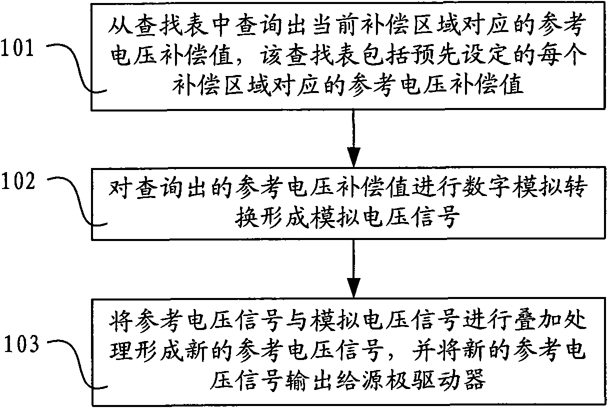
[0022] figure 1 A flow chart of a reference voltage compensation method provided in Embodiment 1 of the present invention, as shown in figure 1 As shown, the method includes:

[0023] Step 101, query the reference voltage compensation value corresponding to the current compensation area from the look-up table, the look-up table includes the preset reference voltage compensation value corresponding to each compensation area;

[0024] Step 102, performing digital-to-analog conversion on the inquired reference voltage compensation value to form an analog voltage signal;

[0025] Step 103 , superimpose the reference voltage signal and the analog voltage signal to form a new reference voltage signal, and output the new reference voltage signal to the source driver.

[0026] In the technical solution of this embodiment, the reference voltage compensation value corresponding to the current compensation area is found from the lookup table, and the analog voltage signal converted fro...


PUM


Abstract

The invention discloses a reference voltage compensating device and method. The method comprises the following steps: 1, inquiring a reference voltage compensating value corresponding to the current compensating region from a look-up table, wherein the look-up table contains preset reference voltage compensating values corresponding to all the compensating regions; 2, carrying out digital-analog conversion on the inquired reference voltage compensating value to form an analog voltage signal; and 3, stacking a reference voltage signal and the analog voltage signal to form a new reference voltage signal, and outputting the new reference voltage signal to a source electrode driver. Because the source electrode driver uses the formed new reference voltage signal in the technical scheme, the problems of image retention and poor image quality of displayed pictures caused by the uneven distribution of common electrode voltage on a liquid crystal panel can be effectively solved, thereby reducing the image retention of displayed pictures and improving the image quality of the displayed pictures.

Description

technical field [0001] The invention relates to the field of liquid crystal display manufacture, in particular to a reference voltage compensation device and method. Background technique [0002] A liquid crystal display usually drives a liquid crystal panel in a progressive scanning manner, and the common electrodes on the liquid crystal panel are driven by a common electrode voltage (Vcom). On the one hand, in order to obtain a larger aperture ratio, the width of the transmission line on the liquid crystal panel needs to be smaller and smaller, which puts forward higher requirements for the manufacturing process of the transmission line. When the width of the manufactured transmission line is inconsistent, the liquid crystal The impedance of the transmission line on the panel will change, which will make the common electrode voltage distribution on the liquid crystal panel uneven. On the other hand, the voltage of the common electrode in the area away from the connection ...

Claims


Application Information

Patent Timeline
Patent Type & Authority Applications(China)
IPC IPC(8): G09G3/36
Inventor 张亮郑喆奎
Owner BEIJING BOE OPTOELECTRONCIS TECH CO LTD
Why Eureka
Try Eureka