Preparation method of Auger electron spectroscopy detection sample

A technology for detecting samples and Auger electrons, applied in measuring devices, material analysis using wave/particle radiation, instruments, etc., can solve problems such as distortion of Auger electron spectrum and inability to obtain Auger electron spectrum, and eliminate Charging effect, the effect of simple and easy operation

Inactive Publication Date: 2011-04-20
SEMICON MFG INT (SHANGHAI) CORP
View PDF0 Cites 3 Cited by
  • Summary
  • Abstract
  • Description
  • Claims
  • Application Information

AI Technical Summary

Problems solved by technology

[0006] The technical problem to be solved in the present invention is to provide a method for preparing a sample for detection by Auger electron spectroscopy, so as to solve the problem that when the detection sample is irradiated by an electron beam, a charging effect is formed on the surface of the sample, resulting in the inability to obtain the desired Auger electron spectrum. Or the problem of distorting the obtained Auger electron spectrum

Method used


Image

  • Preparation method of Auger electron spectroscopy detection sample
  • Preparation method of Auger electron spectroscopy detection sample
  • Preparation method of Auger electron spectroscopy detection sample

Examples


Embodiment Construction

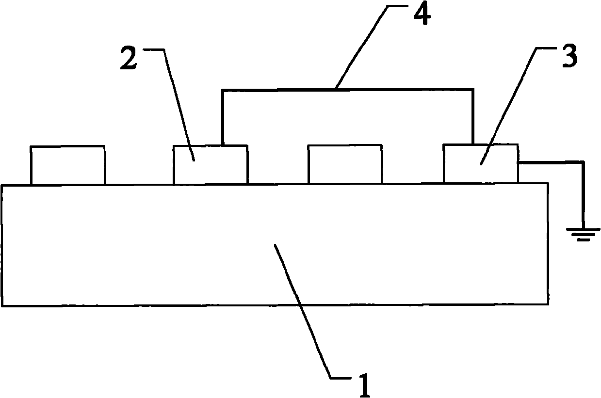
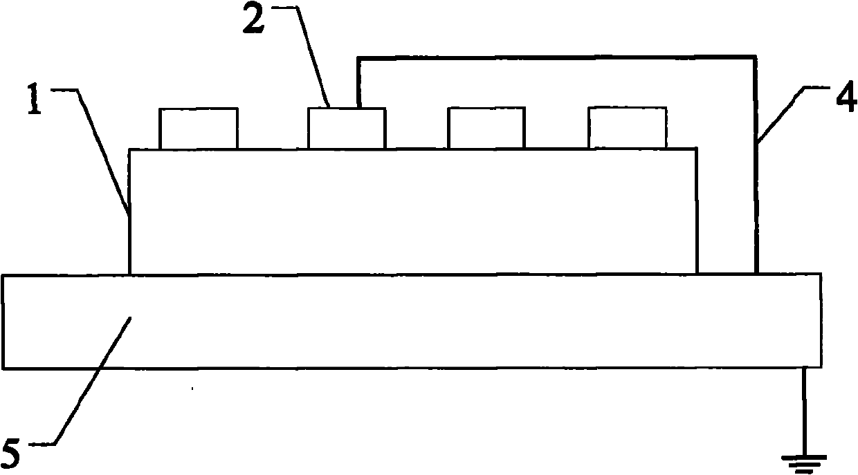
[0022] In order to make the above objects, features and advantages of the present invention more comprehensible, specific implementations of the present invention will be described in detail below in conjunction with the accompanying drawings.

[0023] The preparation method of the Auger electron spectrum detection sample described in the present invention can be realized in various alternative ways, and the following is illustrated by a preferred embodiment. Of course, the present invention is not limited to this specific embodiment. Common substitutions known to those of ordinary skill in the art undoubtedly fall within the protection scope of the present invention.

[0024] Secondly, the present invention is described in detail using schematic diagrams. When describing the embodiments of the present invention in detail, for the convenience of illustration, the schematic diagrams are not partially enlarged according to the general scale, which should not be used as a limitati...


PUM


Abstract

The invention provides a preparation method of an Auger electron spectroscopy detection sample, which comprises the following steps of: providing an original detection sample, wherein the original detection sample comprises a semiconductor substrate, a weld pad arranged on the semiconductor substrate and a passivation layer arranged on the weld pad, the passivation layer is provided with an opening exposing part of the weld pad; and grounding a region to be detected and analyzed on the original detection sample. The preparation method of the Auger electron spectroscopy detection sample can effectively eliminate the charge effect on the surface of the sample during the Auger electron spectroscopy detection though grounding the region to be detected on the sample, thereby obtaining accurate Auger electron spectroscopy. The preparation method of the sample is simple and easy to operate, and can obtain remarkable benefit effects without large-cost input.

Description

technical field [0001] The invention relates to the field of integrated circuit testing, in particular to a method for preparing samples for detection by Auger electron spectroscopy. Background technique [0002] In the field of integrated circuit manufacturing, bonding pads play a very important role in the internal structure of semiconductor devices as a connection between a semiconductor device and another semiconductor device or electronic component to form a receiving component of an electronic circuit module. Therefore, it is required that the pad must have good electrical conductivity and high reliability. Generally, the bonding pad formation process of semiconductor devices includes the following steps: first, forming a conductive layer on the semiconductor substrate, wherein the material of the conductive layer can be one of aluminum or aluminum alloy or a combination thereof; then, etching the conductive layer layer to form a pad pattern; then, a passivation layer...

Claims


Application Information

Patent Timeline
Patent Type & Authority Applications(China)
IPC IPC(8): G01N23/227
Inventor 张启华赵燕丽高强
Owner SEMICON MFG INT (SHANGHAI) CORP
Why Eureka
Try Eureka