Embedded sram structure and chip

一种静态随机存取、存储器芯片的技术,应用在静态存储器、数字存储器信息、信息存储等方向,能够解决装置控制能力及数据稳定性影响等问题,达到提高静态噪声边限及晶体管匹配性、改善可靠度的效果

Active Publication Date: 2011-04-27
TAIWAN SEMICON MFG CO LTD
View PDF4 Cites 22 Cited by
  • Summary
  • Abstract
  • Description
  • Claims
  • Application Information

AI Technical Summary

Problems solved by technology

However, reducing the gate length in order to reduce the transistor pitch will affect the controllability and data stability of the device

Method used


Image

  • Embedded sram structure and chip
  • Embedded sram structure and chip
  • Embedded sram structure and chip

Examples


Embodiment Construction

[0033] The following describes the preferred embodiment of the present invention. Each embodiment is used to illustrate the principles of the present invention, but not to limit the present invention. The scope of the invention should be determined by the terms of the appended claims.

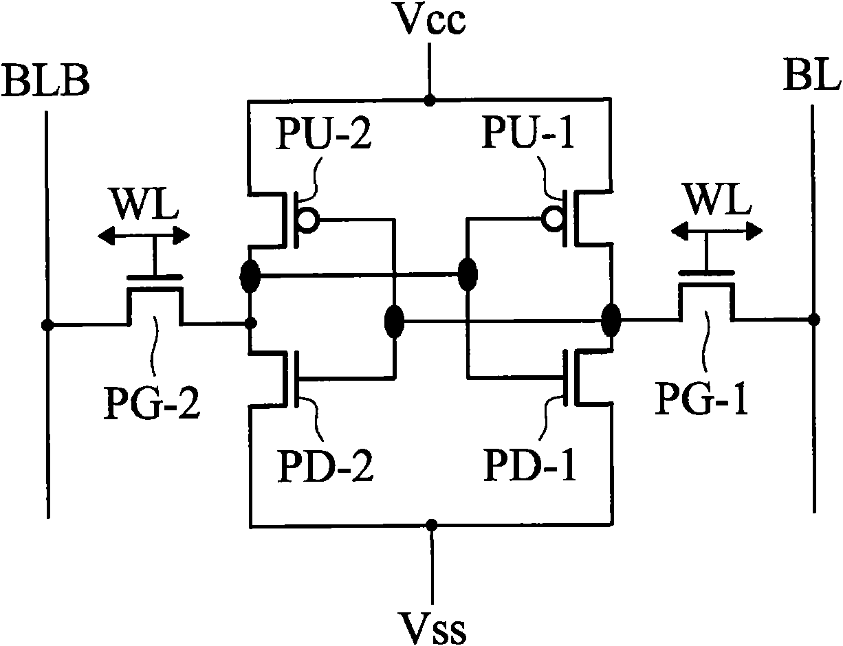
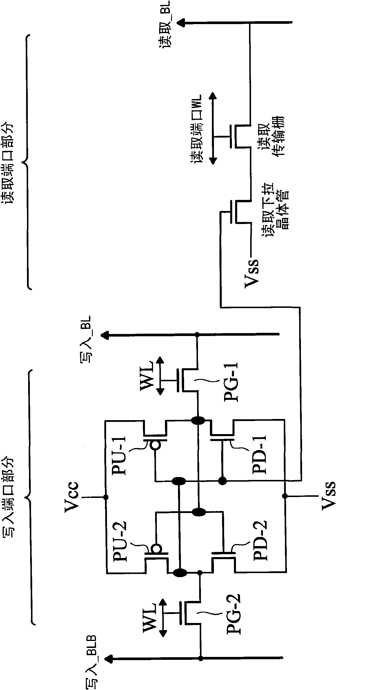
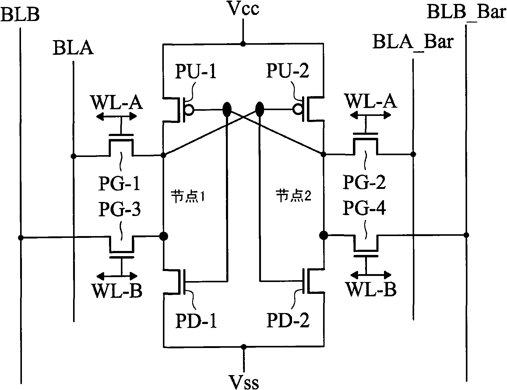
[0034] As used herein, the term "gate poly" refers to any wire capable of forming the gate of a transistor, although the wire can still be a conductive material (eg, metal, metal silicide, metal nitride, or combinations thereof) of amorphous silicon material.

[0035] As is known to those of ordinary skill in the art familiar with SRAM design, one way to measure the performance of an SRAM is to measure its cell array speed. The bit lines are connected to sense amplifiers for signal comparison. The voltage difference between the bit lines BL and BLB determines the speed of the SRAM. There are two ways to improve the BL / BLB differential voltage, one is to increase the lattice current, and the ot...


PUM


Abstract

An embedded Static random access memory (SRAM) chip includes a first SRAM array of first SRAM unit cells. Each first SRAM unit cell includes a data latch for data storage and at least two pass gates for data reading and writing access. The cell area is defined by a first X-pitch and a first Y-pitch, the X-pitch being longer than the Y-pitch. A plurality of logic transistors are formed outside of the first SRAM array, the plurality of logic transistors including at least first and second logic transistor having first and second gate pitches defined between their source and drain contacts. The second gate pitch is the minimum logic gate pitch for the plurality of logic transistors. The first Y-pitch is equal to twice the first gate pitch and the ratio of the first Y-pitch to twice the second logic gate pitch is greater than one. The invention can improve the SER reliability, improve static noise margin and transistor match.

Description

technical field [0001] The present invention generally relates to a semiconductor device, and also relates to a memory lattice, and further relates to the structure and layout design of the static random access memory lattice. Background technique [0002] Static Random Access Memory (SRAM) is often used in integrated circuits. Embedded SRAM is widely used in high-speed communication, image processing and single-chip system (System On Chip, SOC) and other fields. The advantage of the SRAM lattice is that it can retain data without refreshing. Generally, an SRAM cell includes two pass-gate transistors through which one bit of data can be written into or read out of the SRAM. The type of SRAM lattice mentioned above is called a single-port SRAM lattice. Another type of SRAM cell is called a dual port SRAM cell, which includes four pass-gate transistors. Figure 1A , Figure 1B and Figure 1C They are: a six-transistor single-port SRAM lattice circuit, an eight-transistor ...

Claims


Application Information

Patent Timeline
Patent Type & Authority Applications(China)
IPC IPC(8): H01L27/11G11C11/41
CPCH01L27/1104G11C8/16H01L27/0207H01L27/11H01L27/1116H01L27/105H10B10/00H10B10/12H10B10/18
Inventor 廖忠志
Owner TAIWAN SEMICON MFG CO LTD
Why Eureka
Try Eureka