Transistor array substrate
A transistor array and transistor technology, which is applied to electric solid-state devices, semiconductor devices, optics, etc., can solve the problems of increasing production cost and complicated production process, and achieve the effect of eliminating color shift.
Inactive Publication Date: 2011-06-01
华映视讯(吴江)有限公司 +1
View PDF7 Cites 24 Cited by
- Summary
- Abstract
- Description
- Claims
- Application Information
AI Technical Summary
Problems solved by technology
Method used
View moreImage
Smart ImageViewing Examples

Examples
Embodiment Construction
Login to View More PUM
 Abstract
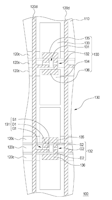
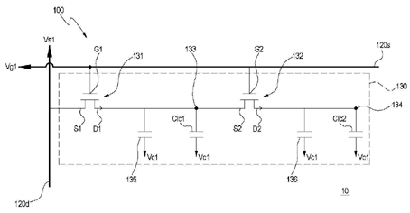
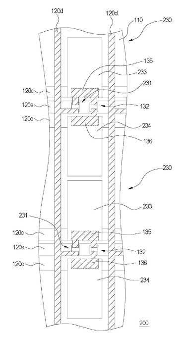
The invention provides a transistor array substrate which comprises a substrate, a plurality of scanning lines, a plurality of data lines and a plurality of pixel units. The scanning lines, the data lines and the pixel units are all arranged on the substrate. Each pixel unit comprises a first transistor, a second transistor, a first pixel electrode, a second pixel electrode, a first storage capacitor and a second storage capacitor. The second transistors and the first transistors are electrically connected with the same scanning line and the same data line, and are connected in series. The first pixel electrodes are electrically connected with the first transistors, while the second pixel electrodes are electrically connected with the second transistors. The first storage capacitors are electrically connected with the first transistors and the second transistors while the second storage capacitors are electrically connected with the second transistors.
Description
technical field [0001] The present invention relates to an active component array substrate, and in particular to a transistor array substrate. Background technique [0002] In today's wide viewing angle liquid crystal display (Liquid Crystal Display, LCD) technology, how to solve the color shift is a very important issue. In detail, the so-called color shift means that the color of the picture of the liquid crystal display changes as the viewing angle changes, causing the display picture to appear white when the viewing angle increases. In order to solve the color shift problem, two methods for improving the color shift have been proposed. One method is to make one more coupling capacitor in a single pixel unit. This coupling capacitor utilizes the effect of voltage coupling to enable the pixel electrode in a single pixel unit to provide electric fields of different sizes. In this way, different arrangements of liquid crystal molecules are generated, which prompts the p...
Claims
Login to View More Application Information
Patent Timeline
 Patent Type & Authority Applications(China)
IPC IPC(8): G02F1/1362G02F1/1368G02F1/1343H01L27/02
Inventor 吴纪良
Owner 华映视讯(吴江)有限公司
Features
- R&D
- Intellectual Property
- Life Sciences
- Materials
- Tech Scout
- Unparalleled Data Quality
- Higher Quality Content
- 60% Fewer Hallucinations
Learn More Browse by: Latest US Patents, China's latest patents, Technical Efficacy Thesaurus, Application Domain, Technology Topic, Popular Technical Reports.
© 2025 PatSnap. All rights reserved.Legal|Privacy policy|Modern Slavery Act Transparency Statement|Sitemap|About US| Contact US: help@patsnap.com