PCB (Printed Circuit Board) grounding structure in flip phone
A PCB board, flip phone technology, applied in the direction of the phone structure and other directions, can solve the problems of destroying the antenna radiation pattern, performance deterioration, and antenna low-frequency radiation performance deterioration, etc., to eliminate the damage and ensure the work performance.
- Summary
- Abstract
- Description
- Claims
- Application Information
AI Technical Summary
Problems solved by technology
Method used
Image

Examples
Embodiment Construction
[0017] The present invention will be described in detail below in conjunction with the accompanying drawings.
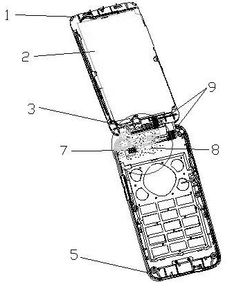
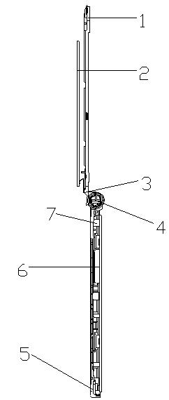
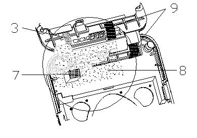
[0018] Such as Figure 1-3 As shown, the flip mobile phone PCB board grounding structure disclosed in this embodiment is to install a metal shrapnel 3 in the upper cover casing, and an elastic spring foot is arranged at both ends of A and B of the metal shrapnel 3, and the A end bounces. The feet are directly in contact with the ground of the display board 2 in the upper cover casing 1 through elastic force. The main board 2 of the display screen is exposed to copper at the contact point area with the spring foot of the A end of the metal shrapnel 3, and the spring foot of the B end of the metal shrapnel 3 is directly in contact with the metal shaft 4 through the action of elastic force. The B-end spring foot of 3 and the contact point area of metal rotating shaft 4 are made through gap. In this way, the ground of the display panel 2 is directly electrically conn...
PUM
 Abstract
Description
Claims
Application Information
 - R&D Engineer
- R&D Manager
- IP Professional
- Industry Leading Data Capabilities
- Powerful AI technology
- Patent DNA Extraction
Browse by: Latest US Patents, China's latest patents, Technical Efficacy Thesaurus, Application Domain, Technology Topic.
© 2024 PatSnap. All rights reserved.Legal|Privacy policy|Modern Slavery Act Transparency Statement|Sitemap