High brightness diode output methods and devices

A technology of output surface and output shaft, which is applied in the direction of laser components, instruments, condenser mirrors, etc., and can solve problems such as brightness loss

Active Publication Date: 2011-06-08
贰陆激光企业有限责任公司
View PDF1 Cites 15 Cited by
  • Summary
  • Abstract
  • Description
  • Claims
  • Application Information

AI Technical Summary

Problems solved by technology

As a result, loss of brightness occ

Method used


Image

  • High brightness diode output methods and devices
  • High brightness diode output methods and devices
  • High brightness diode output methods and devices

Examples


Embodiment Construction

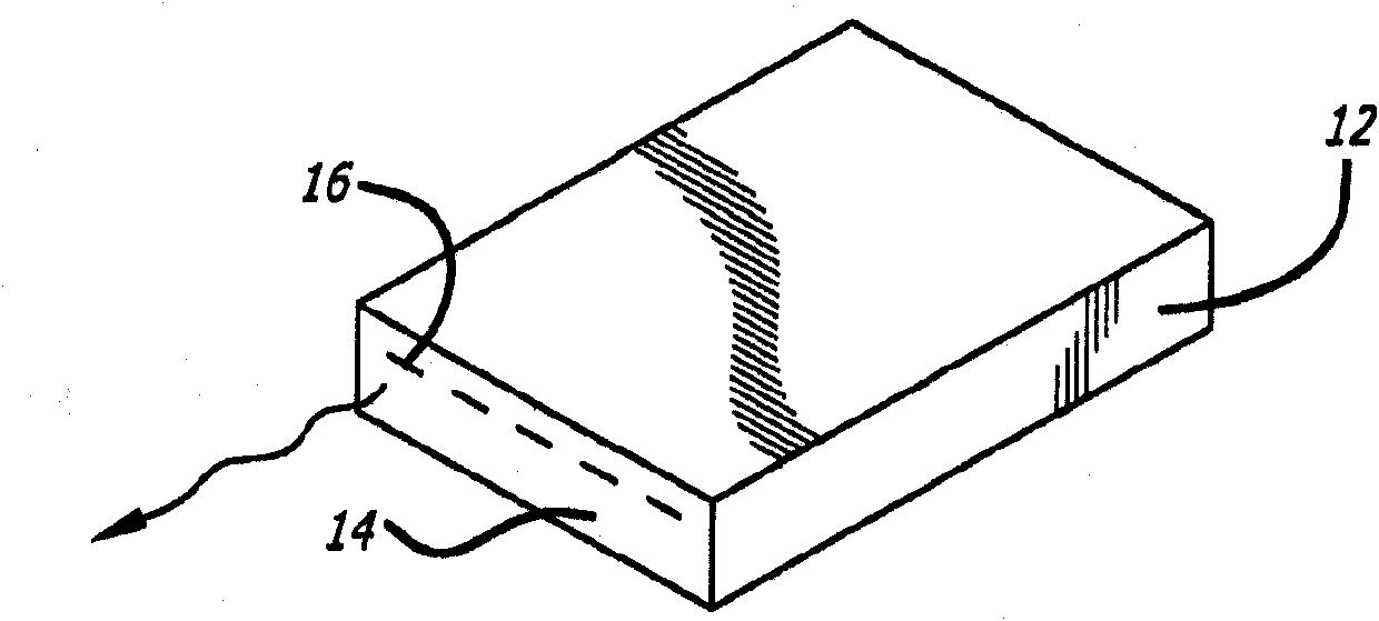
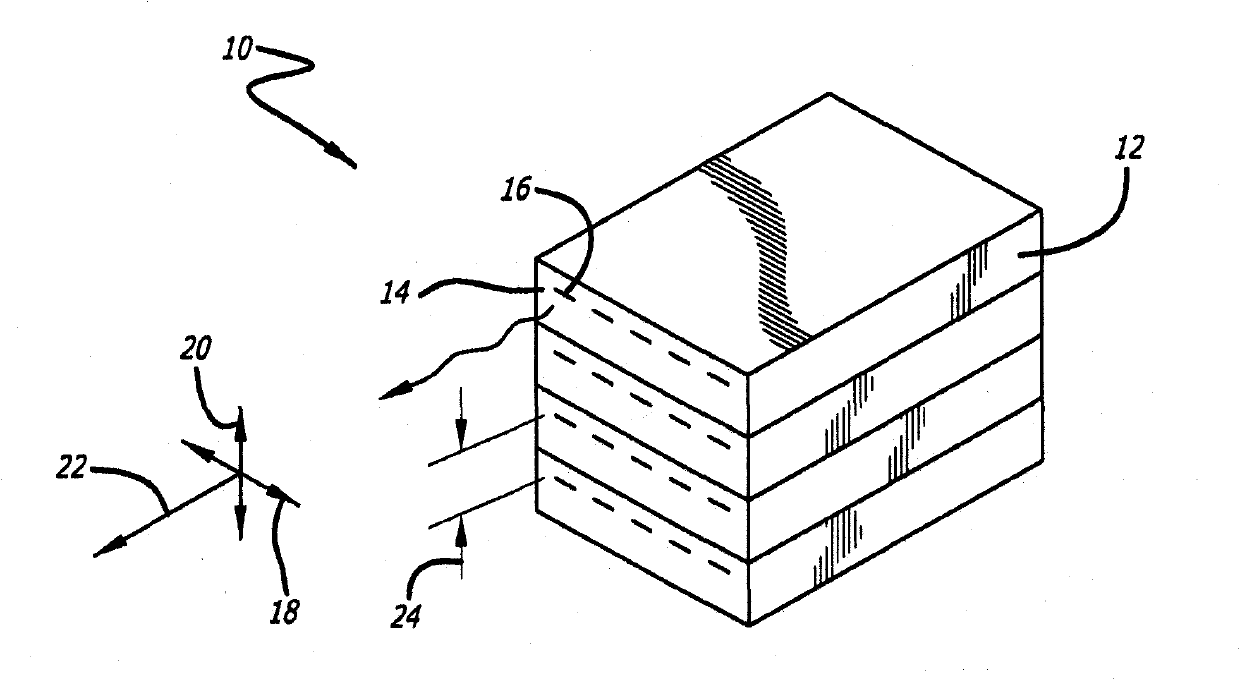
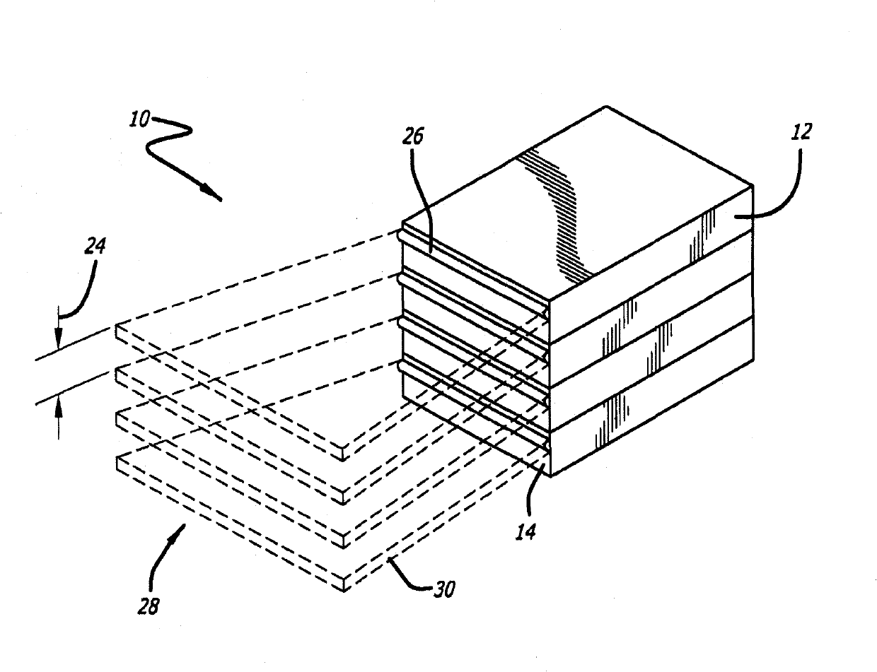
[0045] Embodiments discussed herein relate to methods and apparatus for processing the output of an emitter, such as a laser emitting bar or chip provided with one or more emitters. Embodiments discussed herein also relate to methods and apparatus for coupling the output of a laser emitting bar to a light guide, such as an optical fiber. Such emitting strips or chips may be mounted or incorporated into optical system embodiments by various methods. For such an optical assembly, it is important to properly align the chip's output array and do so with ease and precision, while the resulting structure efficiently dissipates heat generated by the chip. For some embodiments, it is desirable to minimize the number of optical components used in the optical system to save space and cost of the optical system.

[0046] figure 1 A laser emitting bar 12 is shown having an output face 14 comprising a total of 5 emitters 16 with optical axes substantially parallel to each other. Althoug...


PUM


Abstract

Devices and methods for maintaining the brightness of laser emitter bar outputs having multiple emitters for coupling and other applications. In some embodiments, at least one brightness enhancement optic may be used in combination with a beam reformatting optic.

Description

technical field [0001] Optical systems and components thereof may be used to maintain the brightness of an output beam from a laser emitter bar. Some embodiments may be used for efficient coupling of laser emitting bar output beams or other suitable applications. Background technique [0002] For applications that require light energy, or in some cases laser energy, it is advantageous to use a solid-state light source, such as a reliable and relatively cost-effective laser diode that is commonly available on the market as a laser energy source. Such devices may include multiple laser emitters arranged in a single laser bar, which simultaneously emit laser light in the same direction. Additionally, multiple solid state or laser emitting bars can be arranged in a multilayer structure to generate higher power levels. [0003] Laser diode bars are commonly used in communication technology equipment, medical applications or other applications such as military applications where...

Claims


Application Information

Patent Timeline
IPC IPC(8): H01S3/10H01S3/0941H01S3/02
CPCG02B27/30G02B27/0966G02B27/0905G02B27/0961H01S5/4012G02B19/0057H01S5/4025G02B19/0014G02B27/0922G02B19/0028
Inventor 埃德蒙·L·沃拉克奥斯卡·D·罗梅罗詹姆斯·哈里森朴尚锡
Owner 贰陆激光企业有限责任公司
Why Eureka
Try Eureka