Supercharge Your Innovation With Domain-Expert AI Agents!

Exposure device, exposure method and producing method of display panel substrate

A technology of exposure device and exposure method, which is applied in the direction of exposure device for photo-plate-making process, photo-plate-making process for patterned surface, micro-lithography exposure equipment, etc., can solve the problems of time and effort, cost, and unsuitable technology, etc. It achieves the effects of suppressing deviation in the scanning direction, improving drawing accuracy, and uniform light distribution

Inactive Publication Date: 2011-06-15
HITACHI HIGH-TECH CORP
View PDF8 Cites 0 Cited by
  • Summary
  • Abstract
  • Description
  • Claims
  • Application Information

AI Technical Summary

Problems solved by technology

Therefore, it takes a lot of time and effort to correct the error of the relative movement between the beam irradiating device and the chuck, or to adjust the position of the head of each beam irradiating device.
[0012] It can be seen that the above-mentioned existing exposure technology and the manufacturing method of the panel substrate for display obviously still have inconvenience and defects, and urgently need to be further improved.
In order to solve the above-mentioned problems, the relevant manufacturers have tried their best to find a solution, but no suitable design has been developed for a long time, and the general technology has no suitable way to solve the above-mentioned problems. This is obviously a problem. Issues that relevant industry players are eager to solve

Method used


Image

  • Exposure device, exposure method and producing method of display panel substrate
  • Exposure device, exposure method and producing method of display panel substrate
  • Exposure device, exposure method and producing method of display panel substrate

Examples


Embodiment Construction

[0065] In order to further explain the technical means and effects of the present invention to achieve the intended purpose of the invention, the exposure device, the exposure method, and the manufacturing method of the display panel substrate proposed according to the present invention will be described below in conjunction with the accompanying drawings and preferred embodiments. The specific implementation, structure, steps, features and effects thereof are described in detail below.

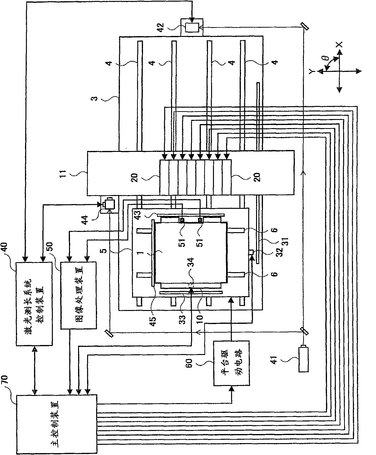
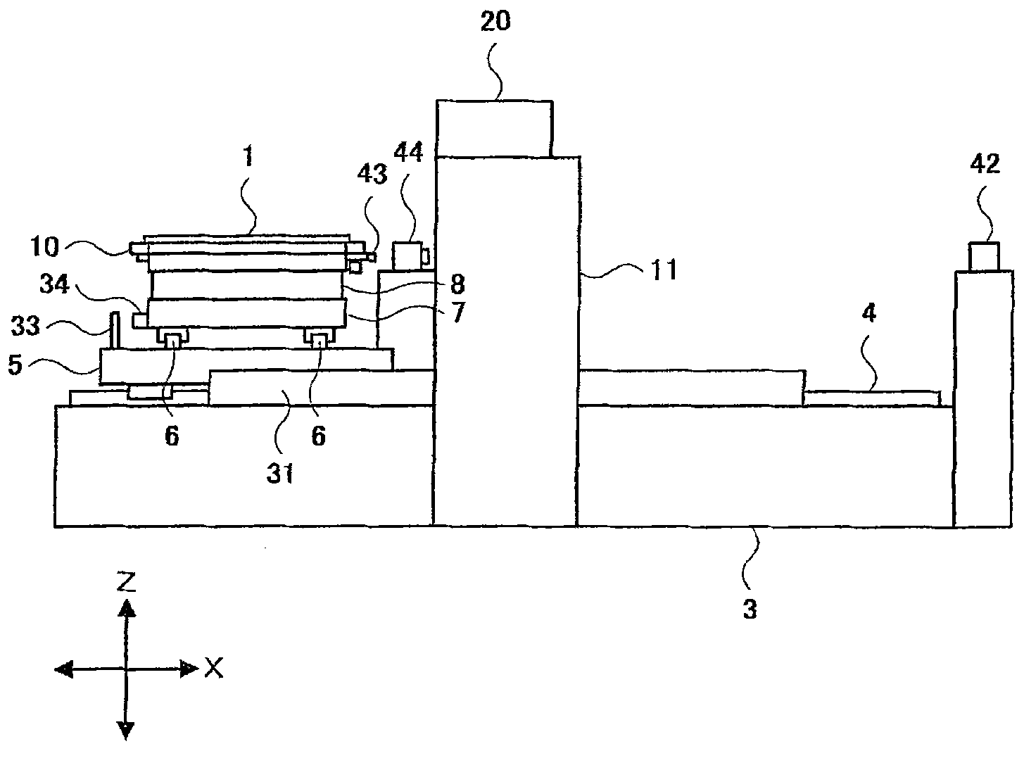
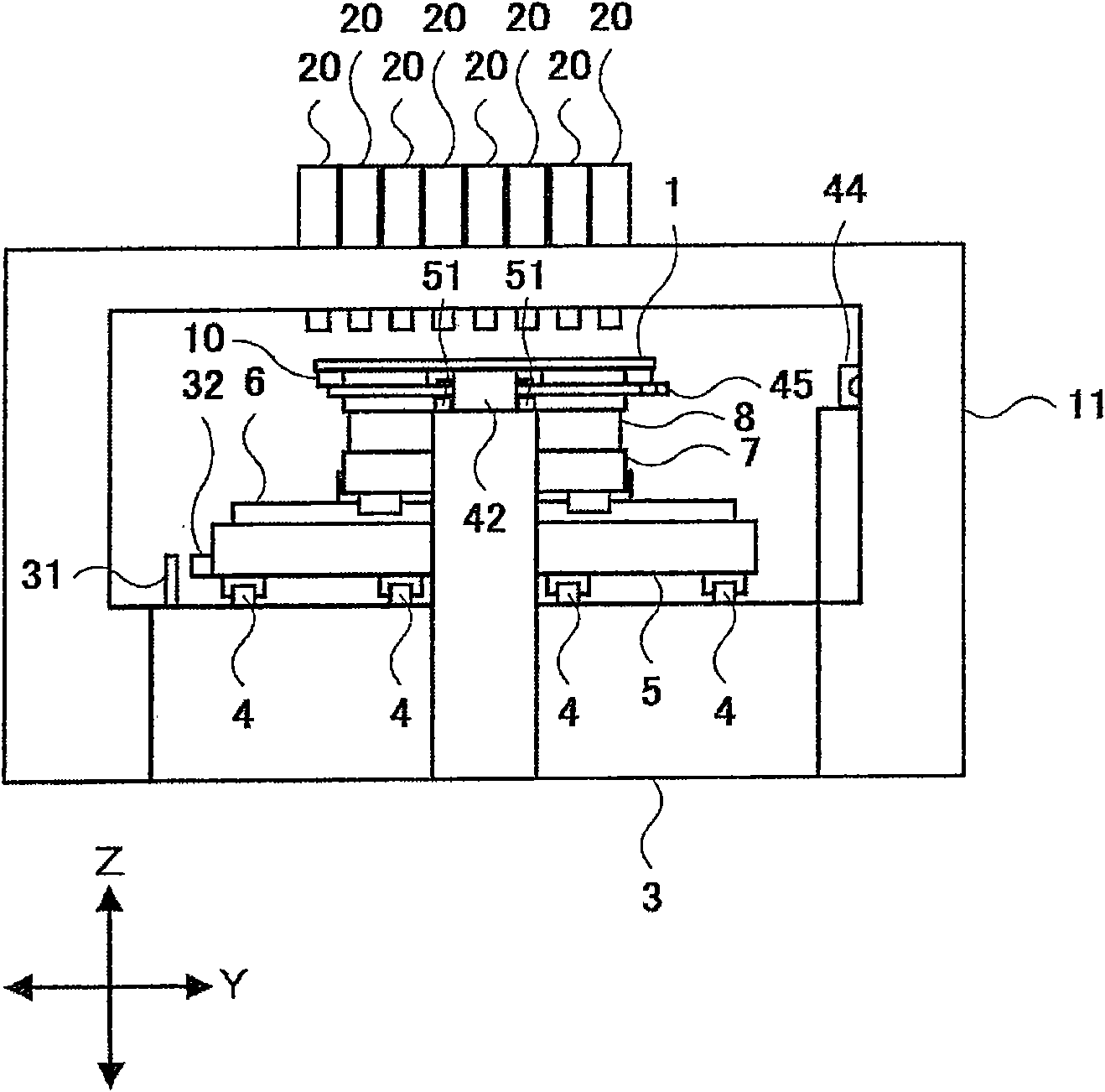
[0066] figure 1 It is a figure which shows the schematic structure of the exposure apparatus which concerns on one Embodiment of this invention. and, figure 2 is a side view of an exposure apparatus according to an embodiment of the present invention, image 3 It is a front view (that is, a front view) of the exposure apparatus which concerns on one Embodiment of this invention. The exposure device includes a base 3, an X guide 4, an X platform 5, a Y guide 6, a Y platform 7, a θ platform ...


PUM


Abstract

The invention relates to an exposure device, an exposure method and a producing method of a display panel substrate. The exposure method comprises the steps of making a chuck (10) and a light beam irradiation device (20) move relatively; supplying a drawing data to a drive circuit (27) of the light beam irradiation device (20). By means of a light receiving mechanism (CCD camera (52)) disposed on the chuck (10), the light beam irradiated from the head part (20a) of the light beam irradiation device (20). Based on the received light beam, the offset of each scanning on the pattern (2) drawn by the light beam can be detected, and the coordinate of the drawing data can be modified based on the detection result. The invention is advantageous in that when the scanning on the substrate by the light beam is conducted for a plurality of times and the pattern is drawn on the substrate, the offset of each scanning can be inhibited and the drawing precision can be increased.

Description

technical field [0001] The present invention relates to a method of irradiating a light beam to a substrate coated with a photo-resist in the manufacture of a display panel substrate such as a liquid crystal display device, and scanning the substrate with the light beam to draw on the substrate. An exposure device for producing a pattern, an exposure method, and a method for manufacturing a display panel substrate using them. In particular, the present invention relates to an exposure device for scanning a light beam to a substrate for multiple times, an exposure method, and a display panel substrate using them manufacturing method. Background technique [0002] Thin Film Transistor (TFT) substrates or color filter (color filter) substrates of liquid crystal display devices used as display panels, substrates for plasma display panels, organic electroluminescence (Electroluminescence, EL ) The manufacture of the substrate for a display panel etc. is carried out by forming a ...

Claims


Application Information

Patent Timeline
IPC IPC(8): G03F7/20H01L21/77
CPCG03F7/2057G03F7/70275G03F7/70291G03F7/70358G03F7/70508G03F7/70558G03F7/70791
Inventor 植原聡原保彦山本健司北村纯一
Owner HITACHI HIGH-TECH CORP
Features
  • R&D
  • Intellectual Property
  • Life Sciences
  • Materials
  • Tech Scout
  • Unparalleled Data Quality
  • Higher Quality Content
  • 60% Fewer Hallucinations
Learn More