Flash memory erase voltage rise control circuit

An erasing voltage and control circuit technology, applied in the field of erasing voltage rising control circuits, can solve the problems of inaccurate erasing voltage rising time and the inability of subsequent circuits to execute accurately and quickly, and achieve the effect of accurate erasing voltage rising time

Active Publication Date: 2015-08-19
SHANGHAI HUAHONG GRACE SEMICON MFG CORP
View PDF3 Cites 0 Cited by
  • Summary
  • Abstract
  • Description
  • Claims
  • Application Information

AI Technical Summary

Problems solved by technology

[0012] In order to overcome the problem that the erasing voltage rise time of the flash memory erasing voltage rise control circuit in the prior art is inaccurate, resulting in the inability to perform accurate and quick subsequent circuit processing, the main purpose of the present invention is to provide a flash memory erasing voltage The rise control circuit, through the negative feedback of the system and the reference current and charging current generated by the supply voltage, avoids the extra current load on the high voltage output of the charge pump, so that the rise time of the erasing voltage is more accurate

Method used


Image

  • Flash memory erase voltage rise control circuit
  • Flash memory erase voltage rise control circuit
  • Flash memory erase voltage rise control circuit

Examples


Embodiment Construction

[0030] The implementation of the present invention is described below through specific examples and in conjunction with the accompanying drawings, and those skilled in the art can easily understand other advantages and effects of the present invention from the content disclosed in this specification. The present invention can also be implemented or applied through other different specific examples, and various modifications and changes can be made to the details in this specification based on different viewpoints and applications without departing from the spirit of the present invention.

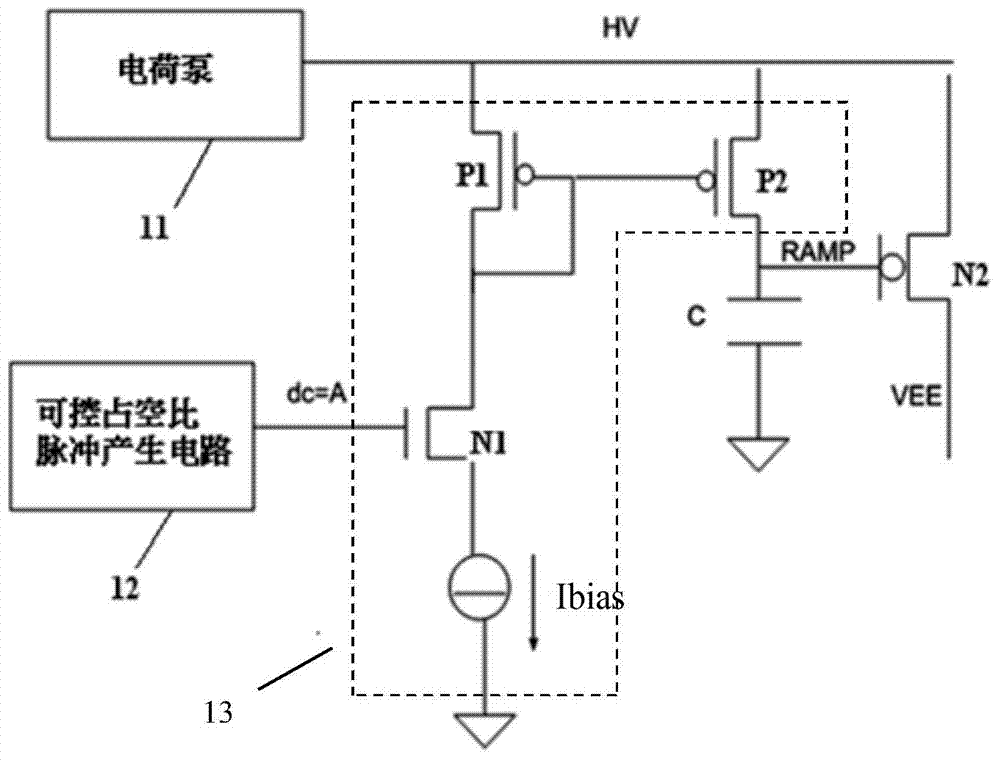
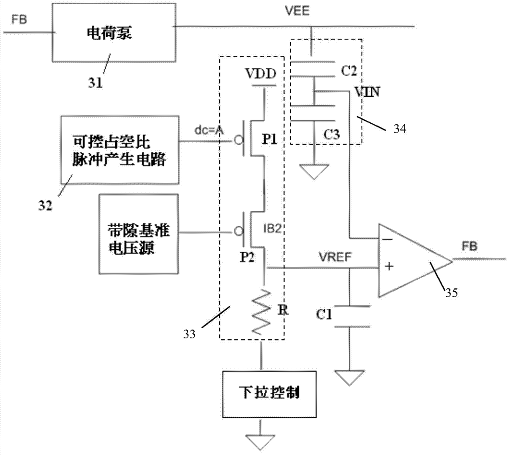
[0031] image 3 It is a circuit diagram of a preferred embodiment of a flash memory erasing voltage rise control circuit of the present invention. like image 3 As shown, an erasing voltage rising control circuit of a flash memory of the present invention at least includes a charge pump 31, a pulse generating circuit 32 with a controllable duty ratio, a reference voltage generating circuit...


PUM


Abstract

The invention discloses an erasing voltage rise control circuit of a flash memory, at least comprising a charge pump, a sampling circuit, a controllable-duty-cycle pulse generating circuit, a reference voltage generating circuit, a first capacitor and a comparison circuit, wherein the charge pump is used for generating an erasing voltage; the sampling circuit is used for sampling the erasing voltage; the controllable-duty-cycle pulse generating circuit is used for generating a pulse with a controllable duty-cycle; the reference voltage generating circuit is connected with a power supply voltage and the controllable-duty-cycle pulse generating circuit so as to generate a reference voltage under the control of the controllable-duty-cycle pulse generating circuit; the first capacitor is connected between the reference voltage generating circuit and the ground; and the comparison circuit is used for comparing a sampling voltage with the reference voltage so as to generate a feedback signal to the charge pump. In the invention, because reference current and charging current are not generated by virtue of high-voltage output of the charge pump, extra current loads can not be generated to the output of the charge pump, no voltage loss is generated, and the rise time of the erasing voltage is more accurate.

Description

technical field [0001] The present invention relates to an erasing voltage rise control circuit, in particular to a flash memory erasing voltage rise control circuit. Background technique [0002] In a flash memory, especially a low-voltage flash memory device, a charge pump (Charge Pump) is often required to generate an erasing voltage. Since the erasing voltage generated by the charge pump without any restrictions often deviates from the required value, in the prior art flash memory, a control circuit is usually set to control the erasing voltage output by the charge pump. [0003] figure 1 It is a circuit structure diagram of an erasing voltage control circuit of a flash memory in the prior art, such as figure 1 As shown, the control circuit includes a charge pump 11, a pulse generation circuit 12 with a controllable duty ratio, a mirror constant current source 13 composed of PMOS transistors P1, P2 and NMOS transistor N1, a capacitor C, and an NMOS transistor N2, where...

Claims


Application Information

Patent Timeline
Patent Type & Authority Patents(China)
IPC IPC(8): G11C16/06G11C16/14
Inventor 杨光军
Owner SHANGHAI HUAHONG GRACE SEMICON MFG CORP
Why Eureka
Try Eureka