Voltage adder circuit and D/A converter circuit
A voltage adder, amplifier circuit technology, used in digital-to-analog converters, amplifiers with semiconductor devices/discharge tubes, amplifiers, etc., can solve problems such as errors
- Summary
- Abstract
- Description
- Claims
- Application Information
AI Technical Summary
Problems solved by technology
Method used
Image
Examples
Embodiment Construction
[0026] Embodiments of the present invention will be described below with reference to the accompanying drawings.
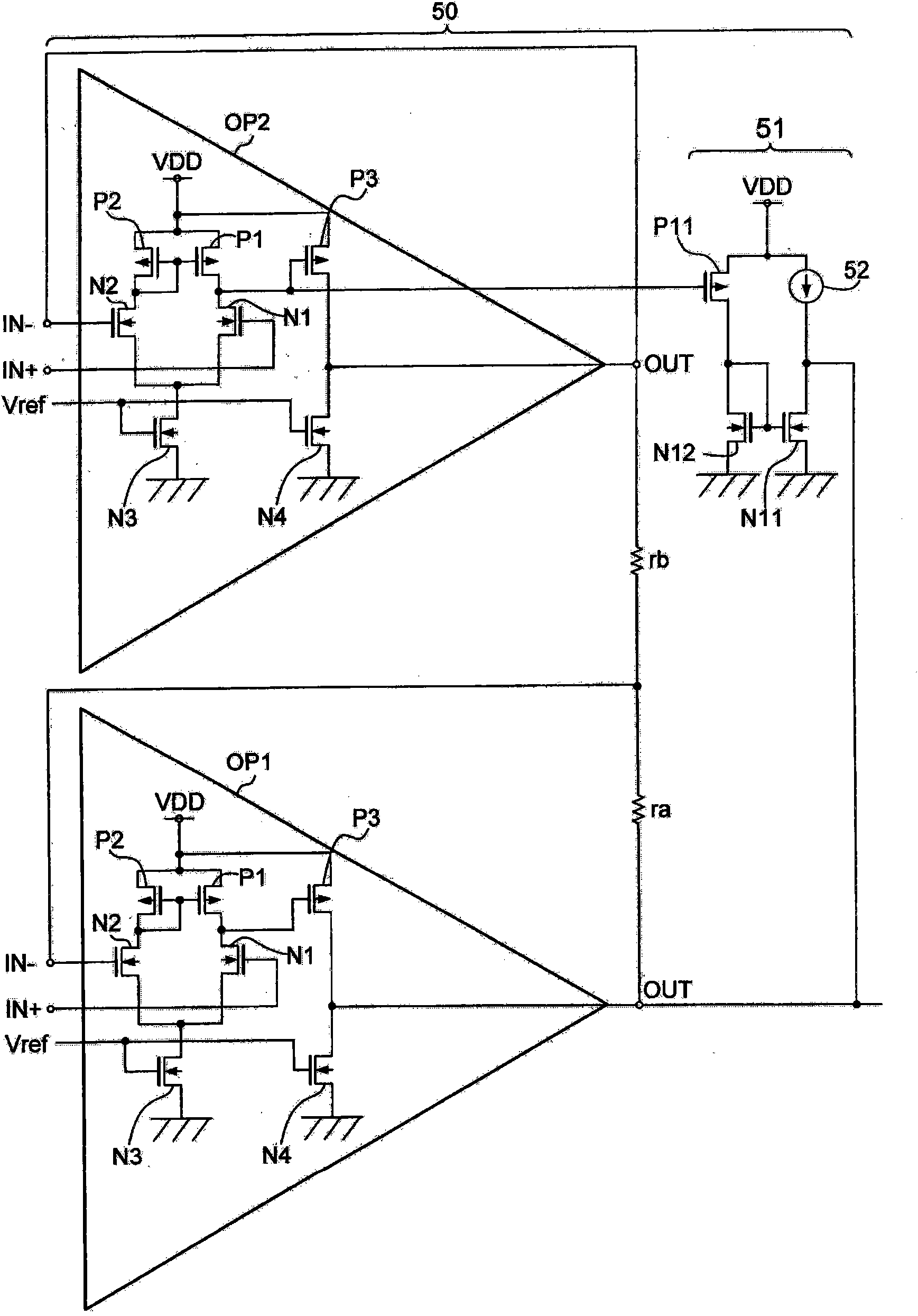
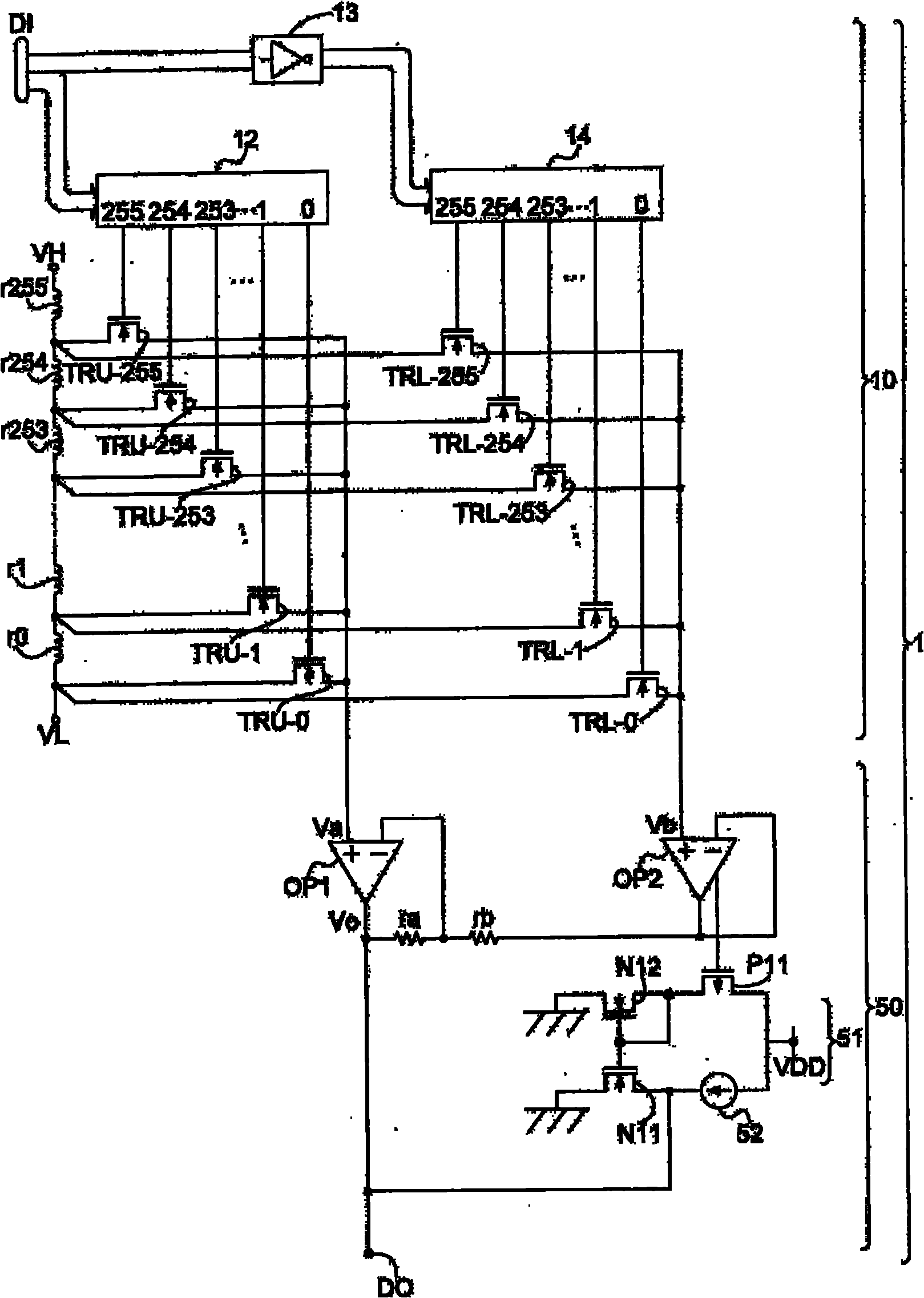
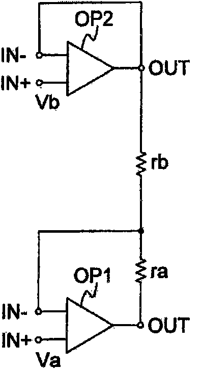
[0027] figure 1 is a view showing the configuration of the voltage adder circuit 50 according to the embodiment of the present invention. The voltage adder circuit 50 performs weighted addition expressed by equation (1) on the voltages Va and Vb supplied from the previous stage circuit, and outputs a voltage Vo as a result of the weighted addition. The voltage adder circuit 50 includes two operational amplifiers OP1 and OP2 , two resistors ra and rb, and a current supply section 51 .
[0028] In the voltage adder circuit 50, the voltage Va is input to the non-inverting input terminal IN+ of the operational amplifier OP1, and the voltage Vb is input to the non-inverting input terminal IN+ of the operational amplifier OP2. The output terminal OUT of the operational amplifier OP1 and the output terminal OUT of the operational amplifier OP2 are connected through resi...
PUM
 Abstract
Description
Claims
Application Information
 - R&D Engineer
- R&D Manager
- IP Professional
- Industry Leading Data Capabilities
- Powerful AI technology
- Patent DNA Extraction
Browse by: Latest US Patents, China's latest patents, Technical Efficacy Thesaurus, Application Domain, Technology Topic, Popular Technical Reports.
© 2024 PatSnap. All rights reserved.Legal|Privacy policy|Modern Slavery Act Transparency Statement|Sitemap|About US| Contact US: help@patsnap.com


