Method and system for judging mask defects

A mask and defect technology, which is applied in the field of mask defect judgment method and judgment system, can solve the problem that it is difficult to fit the mask, and achieve the effect of reducing the probability of defective products

Active Publication Date: 2012-08-22
SEMICON MFG INT (SHANGHAI) CORP +1
View PDF6 Cites 0 Cited by
  • Summary
  • Abstract
  • Description
  • Claims
  • Application Information

AI Technical Summary

Problems solved by technology

However, the non-repeatability of the mask determines the diversity of the graphics environment where the defects on the mask are located. The only few defect inspection settings on the inspection machine are difficult to be suitable for each mask.

Method used


Image

  • Method and system for judging mask defects
  • Method and system for judging mask defects
  • Method and system for judging mask defects

Examples


Embodiment Construction

[0028] The present invention quickly judges whether the mask has a defect and the location of the defect by analyzing the defect position on the wafer, so as to prevent the mask from affecting subsequent wafers and reduce the probability of defective products of the wafer; through the mask defect judgment The system can realize the function of judging the defect of the mask plate online, judge the defect mask plate in time, accurately judge the effect, and improve the judgment efficiency.

[0029] In order to make the above objects, features and advantages of the present invention more obvious and easy to understand, the specific implementation manners of the present invention will be described in detail below in conjunction with the accompanying drawings.

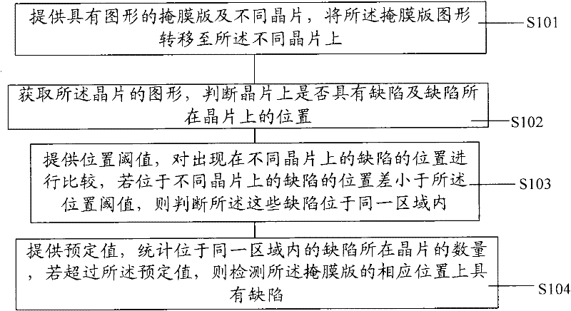
[0030] figure 1 It is a schematic flow chart of a method for judging repetitive defects according to an embodiment of the present invention, including:

[0031] Execute step S101, provide a mask plate with a pattern and a...


PUM


Abstract

The invention relates to a method for judging mask defects, which comprises providing a mask with graphs and different wafers, and transferring the graphs of the mask to different wafers; acquiring the graphs of the wafers, and judging whether the wafers have defects or not and judging the positions at which the defects are positioned on the wafers; providing a position threshold value, comparingthe positions of the defects positioned on different wafers, and if the position difference of defects positioned on different wafers is less than the position threshold value, determining that the defects are positioned in the same area; and providing a preset value, if the number of the wafers in which the defects within the same area are positioned exceeds the preset value, determining that the defects occur on the corresponding position of the mask. The invention also provides a system for judging the mask defects, which realizes the function of judging the defects of the mask on line so as to judge the mask with the defects in time with accurate judging effect and high judging efficiency.

Description

technical field [0001] The invention relates to a semiconductor manufacturing process, in particular to a method and system for judging a mask plate defect. Background technique [0002] In the field of semiconductor manufacturing, photolithography is an important process for forming integrated circuit patterns. The process includes: first coating a layer of photoresist on the die, then exposing a mask with a reference pattern in a photolithography device, and transferring the reference pattern on the mask to the photoresist. Finally, the developer reacts with the photoresist to form a corresponding pattern on the wafer. [0003] As a reference pattern in the lithography process, the mask plays an important role in the lithography and subsequent processes. Fiducial patterns are destroyed when contamination or damage occurs on the reticle. The destroyed reference pattern will be transferred to tens of thousands of wafers through exposure, development and subsequent etching...

Claims


Application Information

Patent Timeline
Patent Type & Authority Patents(China)
IPC IPC(8): G03F1/44H01L21/00G01N21/88
CPCG03F1/84G01N2021/8877G01N21/8851G01N21/956G01N21/9501
Inventor 林光启康栋王永刚张宇磊
Owner SEMICON MFG INT (SHANGHAI) CORP
Why Eureka
Try Eureka