Encapsulation structure of light-emitting diode (LED) and manufacturing method thereof
A technology of light-emitting diodes and light-emitting structures, applied to electrical components, circuits, semiconductor devices, etc., can solve problems such as lengthy time, increased opportunities for defective products, and numerous steps, and achieve the effect of simple manufacturing process and reduced opportunities for defective products
- Summary
- Abstract
- Description
- Claims
- Application Information
AI Technical Summary
Problems solved by technology
Method used
Image

Examples
Embodiment Construction
[0030] The present invention will be further described in detail below in conjunction with the accompanying drawings.
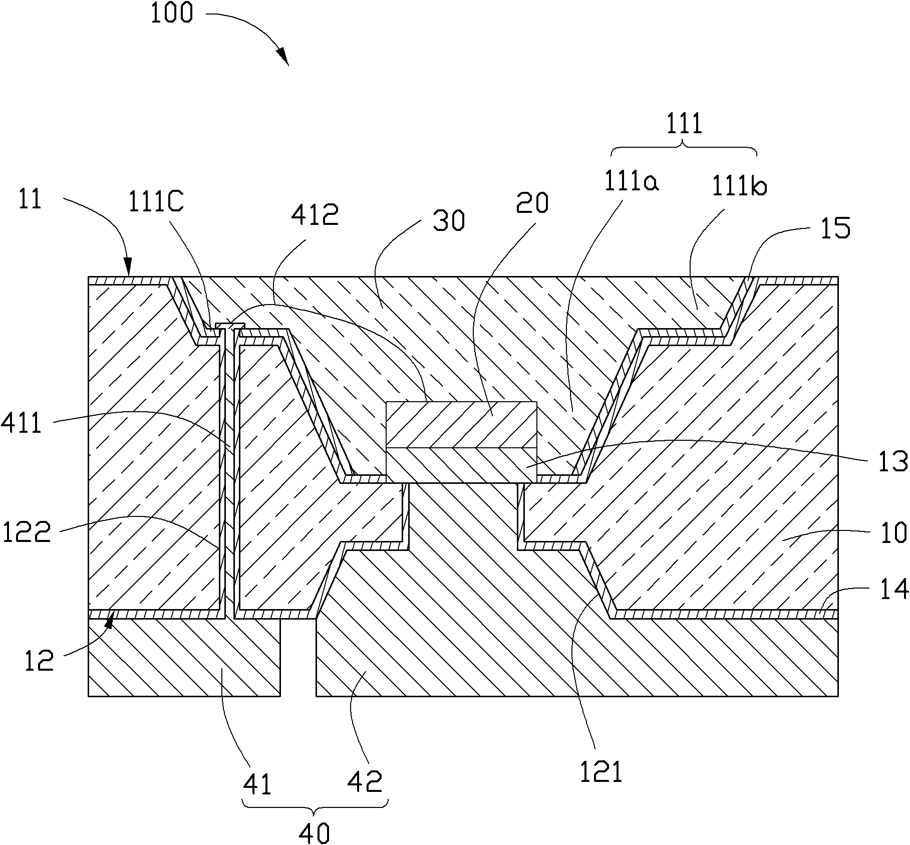
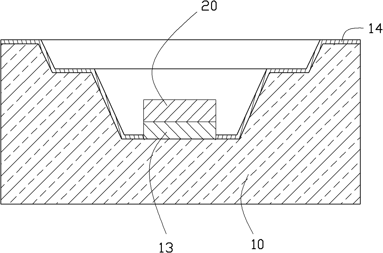
[0031] see figure 1 A light emitting diode packaging structure 100 provided in an embodiment of the present invention includes a substrate 10 , a light emitting structure 20 , a packaging glue 30 and a circuit structure 40 .
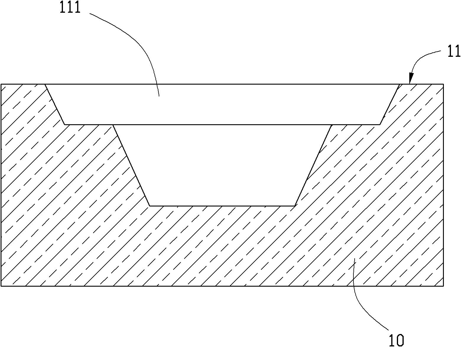
[0032] The substrate 10 has a first surface 11 and a second surface 12 opposite to the first surface 11 . In this embodiment, a first groove 111 is formed on the first surface 11, and the first groove 111 is a stepped groove, which includes a first accommodating portion 111a and a second accommodating portion 111b. A stepped surface 111c is formed between the first accommodating portion 111a and the second accommodating portion 111b, and the stepped surface 111c is substantially parallel to the first surface 11 . Preferably, both the first accommodating portion 111a and the second accommodating portion 111b are trumpet-shaped to facil...
PUM
 Abstract
Description
Claims
Application Information
 - R&D
- Intellectual Property
- Life Sciences
- Materials
- Tech Scout
- Unparalleled Data Quality
- Higher Quality Content
- 60% Fewer Hallucinations
Browse by: Latest US Patents, China's latest patents, Technical Efficacy Thesaurus, Application Domain, Technology Topic, Popular Technical Reports.
© 2025 PatSnap. All rights reserved.Legal|Privacy policy|Modern Slavery Act Transparency Statement|Sitemap|About US| Contact US: help@patsnap.com