
Luminous unit and device of semiconductor laser diode

A technology of laser diodes and light-emitting units, applied in semiconductor lasers, laser parts, lasers, etc., can solve the problems of low threshold, small fluctuation of rated current, reduced working life, etc., and achieve the effect of improving COD threshold and optimizing thickness

Inactive Publication Date: 2012-06-27
INST OF SEMICONDUCTORS - CHINESE ACAD OF SCI
View PDF0 Cites 0 Cited by
  • Summary
  • Abstract
  • Description
  • Claims
  • Application Information

AI Technical Summary

Problems solved by technology

[0003] In the process of realizing the present invention, the inventor realized that the prior art has the following technical defects: the thinner waveguide layer makes the reliability of the 808-HP LDA relatively weak under harsh working environments
Weak reliability is mainly reflected in: the threshold of Catastrophic Optical Damage (COD) is low, and the tolerable rated current fluctuation is not large; while the working life of 808-HP LDA will be significantly reduced due to the occurrence of COD

Method used


Image

  • Luminous unit and device of semiconductor laser diode
  • Luminous unit and device of semiconductor laser diode
  • Luminous unit and device of semiconductor laser diode

Examples


Embodiment Construction

[0022] In order to make the object, technical solution and advantages of the present invention clearer, the present invention will be described in further detail below in conjunction with specific embodiments and with reference to the accompanying drawings.

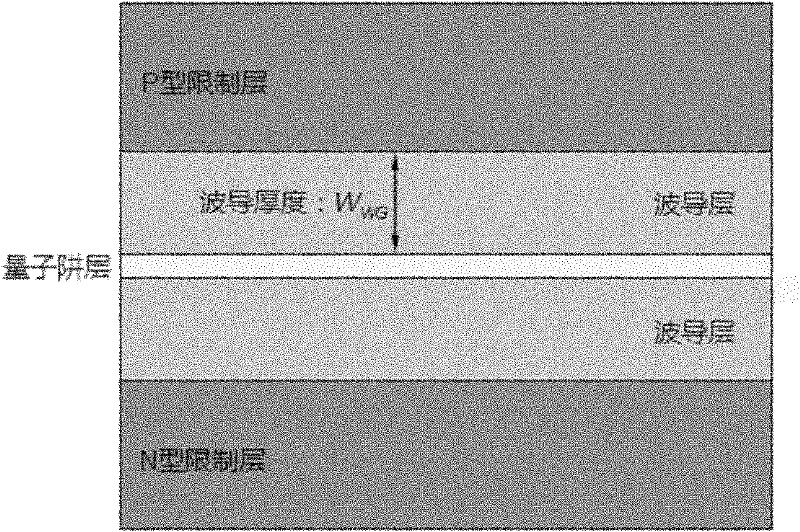
[0023] In an exemplary embodiment of the present invention, a semiconductor laser diode light emitting unit is provided. The output laser power of the light emitting unit is greater than 0.2W. figure 1 It is a schematic structural diagram of a semiconductor laser diode light emitting unit according to an embodiment of the present invention. Such as figure 1 As shown, the structure of the light-emitting unit includes from bottom to top: a first confinement layer, a first waveguide layer, a quantum well layer, a second waveguide layer and a second confinement layer, wherein: the first confinement layer and the second confinement layer are used It is used to form a PN junction for carrier input; the thickness of the first ...


PUM


Abstract

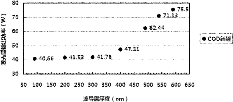
The invention discloses a luminous unit and a luminous device of a semiconductor laser diode. The power of the output laser of the luminous unit is more than 0.2W. The structure of the luminous unit comprises a first limiting layer, a first waveguide layer, a quantum well layer, a second waveguide layer and a second limiting layer from bottom to top, wherein the first limiting layer and the second limiting layer are used for forming a PN junction to perform current carrier input; the thicknesses of the first waveguide layer and the second waveguide layer are between 400 and 600 nanometers, and the first waveguide layer and the second waveguide layer are used for forming a laser transmission channel; and the quantum well layer serving as an active area generates laser. By increasing the thicknesses of the waveguide layers in the luminous unit, the catastrophic optical damage (COD) threshold value of the semiconductor laser diode can be effectively improved.

Description

technical field [0001] The invention relates to the technical fields of microelectronics and optics, in particular to a high-power semiconductor laser diode light-emitting unit and a semiconductor laser diode device. Background technique [0002] In the prior art, the waveguide thickness of the 808nm high-power semiconductor laser diode array (High Power Laser Diode Array, HP LDA for short) is generally about tens of nanometers in consideration of the influence of its photoelectric characteristics. [0003] In the process of realizing the present invention, the inventor realized that the prior art has the following technical defects: the thinner waveguide layer makes the reliability of the 808-HP LDA relatively weaker in harsh working environments. Weak reliability is mainly reflected in: the threshold of photocatastrophic optical damage (COD) is low, and the tolerable rated current fluctuation is not large; while the working life of 808-HP LDA will be significantly reduced ...

Claims


Application Information

Patent Timeline
Patent Type & Authority Patents(China)
IPC IPC(8): H01S5/20H01S5/343
Inventor 郑凯王俊熊聪马骁宇
Owner INST OF SEMICONDUCTORS - CHINESE ACAD OF SCI
Learn More