Method and structure for filling clearances among stacked multi-layer wafers

A technology of multi-layer wafers and stacked structures, which is applied in the manufacture of electrical components, electrical solid devices, semiconductor/solid devices, etc. It can solve the problems of height difference and inability to dispense and fill, so as to avoid short circuits and improve production efficiency.

Inactive Publication Date: 2011-08-10
POWERTECH TECHNOLOGY
View PDF0 Cites 9 Cited by
  • Summary
  • Abstract
  • Description
  • Claims
  • Application Information

AI Technical Summary

Problems solved by technology

[0007] The main purpose of the present invention is to overcome the defects of existing filling method and structure of multilayer wafer stacking gap, and provide a new filling method and structure of multilayer wafer stacking gap. The technical problem to be solv

Method used


Image

  • Method and structure for filling clearances among stacked multi-layer wafers
  • Method and structure for filling clearances among stacked multi-layer wafers
  • Method and structure for filling clearances among stacked multi-layer wafers

Examples


Embodiment Construction

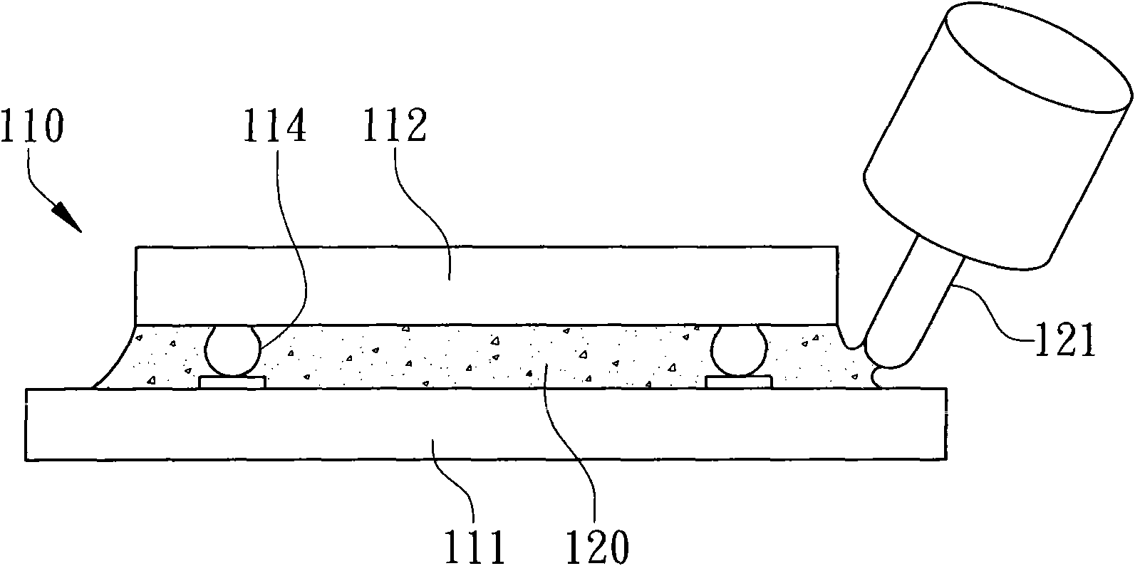
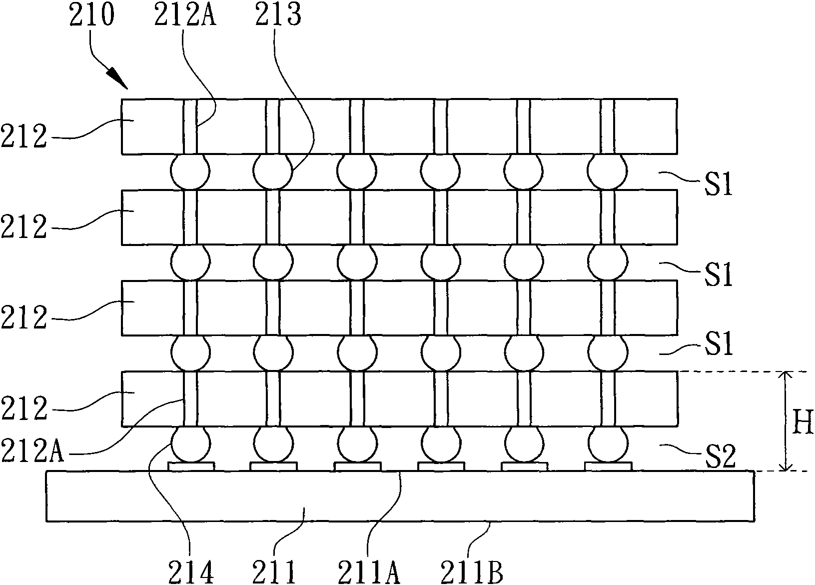
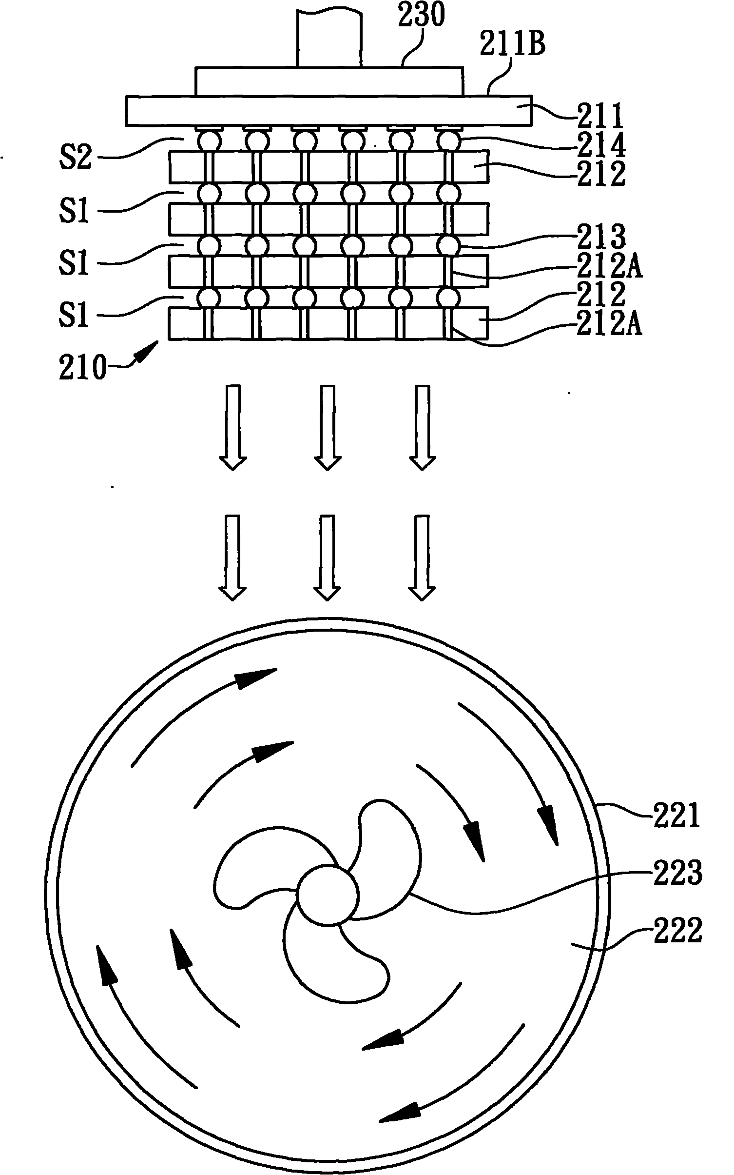
[0053] In order to further explain the technical means and effects of the present invention to achieve the intended purpose of the invention, the specific implementation methods, The method, steps, structure, features and effects thereof are described in detail below.

[0054] Some embodiments of the present invention will be described in detail as follows. However, in addition to the following descriptions, the present invention can also be widely implemented in other embodiments, and the protection scope of the present invention is not limited by the embodiments, which shall prevail by the protection scope of the claims. Moreover, in order to provide a clearer description and an easier understanding of the present invention, various parts in the drawings have not been drawn according to their relative sizes, and some dimensions have been exaggerated compared with other relevant dimensions; irrelevant details have not been completely drawn. are drawn for the sake of simplici...


PUM


Abstract

The invention discloses a method and a structure for filling clearances among stacked multi-layer wafers. According to the method, a wafer stacking structure is provided. The wafer stacking structure comprises a substrate and a plurality of wafers which are stacked on the substrate vertically. At least one primer clearance is formed between any two stacked wafers, and a height difference is formed between the primer clearance and the substrate. Then, the wafer stacking structure is overturned, and the wafers of the wafer stacking structure are dipped into an underfill material, wherein the underfill material is stored in an underfill material storage tank and keeps flowing to fill in the primer clearance. Finally, the wafer stacking structure is taken out and heated to solidify the underfill material in the primer clearance. Therefore, the problem that the clearances among the conventional stacked multi-layer wafers cannot be filled by dispensing can be solved, and a plurality of primer clearances can be filled once, so that production efficiency is improved greatly.

Description

technical field [0001] The invention relates to a manufacturing technology of a semiconductor device, in particular to a method and structure for filling gaps in multilayer wafer stacks. Background technique [0002] During drop and reliability tests of current flip chip or Wafer Level Chip Scale Package (WL-CSP) products, the solder joints between the chip and the substrate are susceptible to drastic changes in external force and thermal stress Fracture damage occurs, which in turn causes damage to the IC chip or failure of internal electrical connections, so it is necessary to use an underfill material to seal and protect the solder joints. The traditional method of forming underfill is to dispense glue on the side of the substrate, heat the substrate properly to make the underfill fluid, and use capillary phenomenon to make the underfill flow into the gap between the IC chip and the substrate. [0003] In advanced packaging technology, the three-dimensional stacking of m...

Claims


Application Information

Patent Timeline
IPC IPC(8): H01L21/50H01L25/00
CPCH01L2224/92125H01L2224/73204
Inventor 徐宏欣简维志
Owner POWERTECH TECHNOLOGY
Why Eureka
Try Eureka