Core burying method for high-current magnetic device and printed circuit board manufacturing method

A printed circuit board and magnetic device technology, applied in the electronic field, can solve the problems of unfavorable power module miniaturization, tight device layout, and occupation of PCB surface space

Inactive Publication Date: 2011-08-17
HUAWEI MACHINERY
View PDF6 Cites 20 Cited by
  • Summary
  • Abstract
  • Description
  • Claims
  • Application Information

AI Technical Summary

Problems solved by technology

[0003] In the process of realizing the embodiment of the present invention, the inventors found the following technical problems in the prior art: the independent surface-mounted magnetic device and the magnetic device of the single-board PCB buckle magnet scheme are all located on the surface of the PCB, and the magnetic device is the height of the power module. The tallest device takes up a lot of PCB surface space, which makes the layout of other components of the power module tight, which is not conducive to the miniaturization of the power module

Method used


Image

  • Core burying method for high-current magnetic device and printed circuit board manufacturing method
  • Core burying method for high-current magnetic device and printed circuit board manufacturing method
  • Core burying method for high-current magnetic device and printed circuit board manufacturing method

Examples


Embodiment Construction

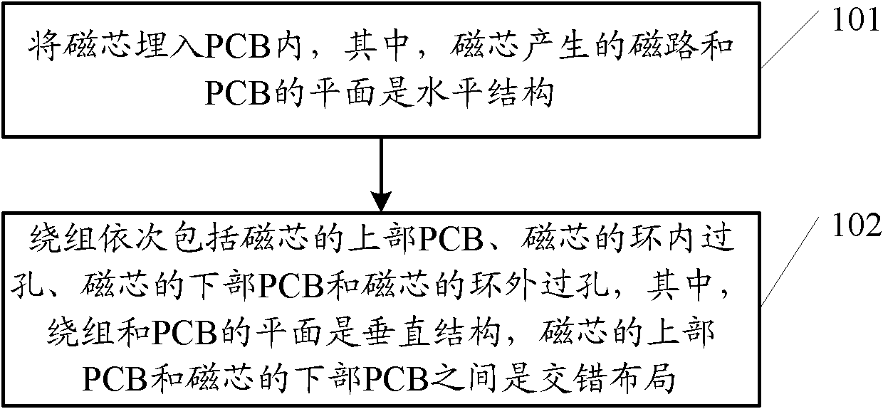
[0026] Embodiments of the present invention provide a magnetic embedding method for a high-current magnetic device and a manufacturing method for a printed circuit board, which are used to save surface space of a PCB and realize miniaturization of a power module.

[0027] In order to make the purpose, features and advantages of the present invention more obvious and understandable, the technical solutions in the embodiments of the present invention will be clearly and completely described below in conjunction with the accompanying drawings in the embodiments of the present invention. Obviously, the following The described embodiments are only some, not all, embodiments of the present invention. All other embodiments obtained by those skilled in the art based on the embodiments of the present invention belong to the protection scope of the present invention.

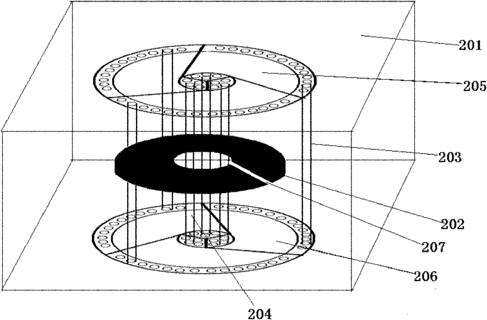
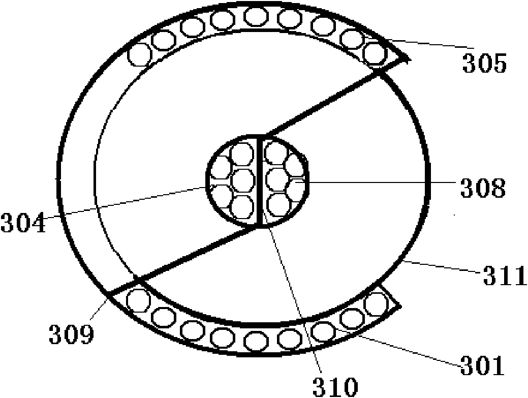
[0028] For a method for embedding magnetization of a large current magnetic device provided in an embodiment of the pre...


PUM


Abstract

The embodiment of the invention discloses a core burying method for a high-current magnetic device and a printed circuit board manufacturing method. The embodiment of the invention can bury a core and a winding into a printed circuit board (PCB) so as to save a surface space of the PCB and realize the miniaturization of a power module. The core burying method of the embodiment of the invention comprises the following step of: burying the core into the PCB, wherein a magnetic circuit produced by the core and a plane of the PCB form a horizontal structure; a winding sequentially comprises an upper PCB of the core, in-ring through holes, a lower PCB of the core, and outside-ring through holes; the winding and the plane of the PCB form a vertical structure; and the upper PCB and lower PCB of the winding are arranged in a staggering way.

Description

technical field [0001] The invention relates to the field of electronic technology, in particular to a magnetic embedding method of a large current magnetic device and a manufacturing method of a printed circuit board. Background technique [0002] With the increase in the integration of electronic products, the miniaturization requirements for power modules are getting higher and higher, which makes it necessary to reduce the layout space of devices. As the core components of power modules, magnetic devices account for about 30-40% of power modules. Printed circuit board (PCB, Printed Circuit Board) space has become a key factor restricting the miniaturization of power modules. At present, there are mainly two types of magnetic device application technologies commonly used in power modules: independent surface-mounted magnetic devices and single-board PCB buckle magnetic solutions. Among them, the independent surface-mounted magnetic Layer-to-layer interconnection forms a ...

Claims


Application Information

Patent Timeline
Patent Type & Authority Applications(China)
IPC IPC(8): H05K3/30H05K1/18
Inventor 李贤明
Owner HUAWEI MACHINERY
Why Eureka
Try Eureka