Pixel clock generator and image forming apparatus

一种像素时钟、生成器的技术,应用在永久直观显示的装置、仪器、图像通信等方向,能够解决光源误差、平均扫描速度误差、非线性误差等问题,达到抑制高频抖动、增加控制带宽的效果

Active Publication Date: 2011-08-17
RICOH KK
View PDF15 Cites 5 Cited by
  • Summary
  • Abstract
  • Description
  • Claims
  • Application Information

AI Technical Summary

Problems solved by technology

[0009] (2) Error due to fluctuation of average scanning speed
[0012] (3) The error of each light source
[0026] (5) Nonlinear error
[0036] In conventional techniques, the control bandwidth cannot be increased to stably control a system with a dead time of one sampling time (e.g., for stable control, the control bandwidth can only be increased up to about a few tenths to one tenth of the sampling frequency)
Therefore, there is a problem that high-frequency jitter of several tens of cycles cannot be sufficiently suppressed

Method used


Image

  • Pixel clock generator and image forming apparatus
  • Pixel clock generator and image forming apparatus
  • Pixel clock generator and image forming apparatus

Examples


no. 1 example

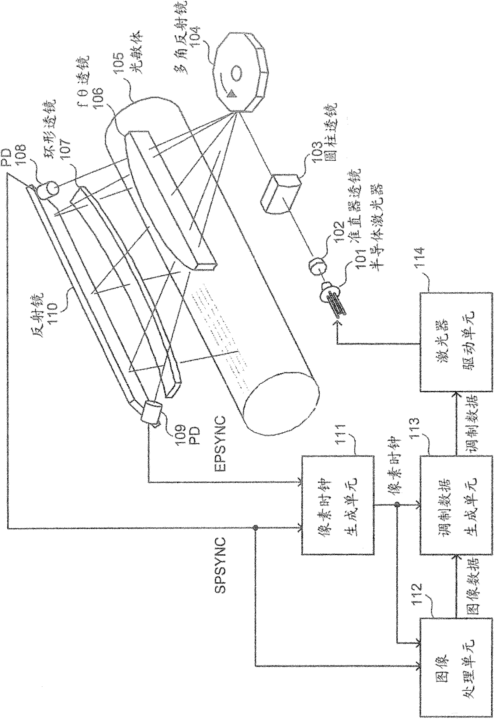
[0090] Such as figure 1 As shown, the imaging device according to this embodiment includes a semiconductor laser 101, a collimator lens 102, a cylindrical lens 103, a polygon mirror 104, a photosensitive element 105, an fθ lens 106, a ring lens 107, a photodetector (hereinafter referred to as “PD”) 108 and 109 , mirror 110 , pixel clock generation unit 111 , image processing unit 112 , modulation data generation unit 113 , and laser drive unit 114 .

[0091] In the present embodiment, the collimator lens 102, the cylindrical lens 103, the polygon mirror 104, the fθ lens 106, the annular lens 107, and the mirror 110 form the optical scanner of the present invention.

[0092] Laser light (beam) output from a semiconductor laser 101 as a light source passes through a collimator lens 102 and a cylindrical lens 103 to be shaped. The laser light enters the polygon mirror 104 as a polarizer, which is provided with a plurality of deflection reflection surfaces (hereinafter, simply r...

no. 2 example

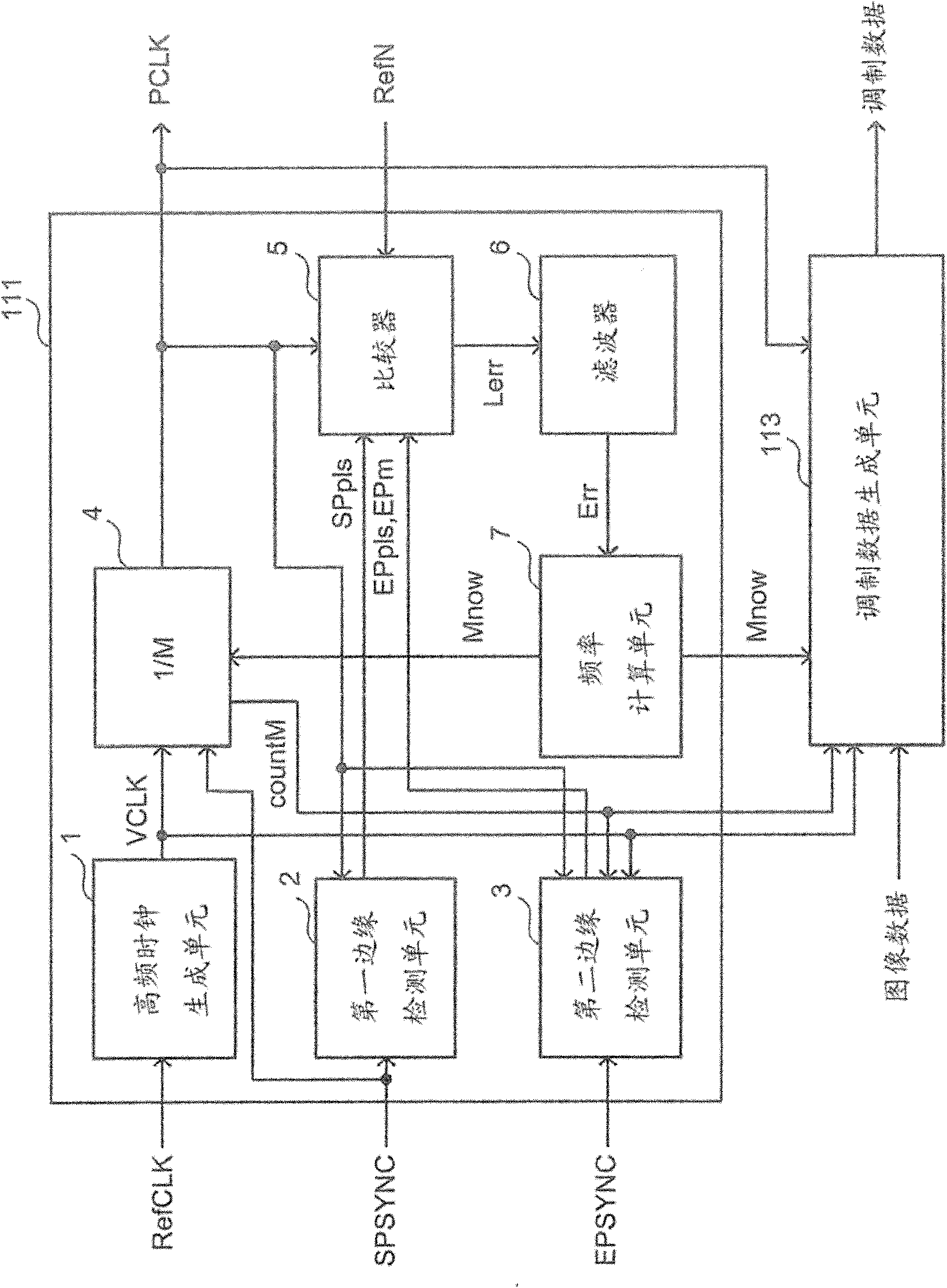
[0229] Such as Figure 15 As shown, the second embodiment differs from the first embodiment in that a pixel clock generation unit 211 is included instead of the pixel clock generation unit 111 .

[0230] The pixel clock generation unit 211 differs from the pixel clock generation unit 111 according to the first embodiment of the present invention in that it includes a frequency calculation unit 8 instead of the frequency calculation unit 7 , and further includes a frequency modulation data generation unit 9 . In other words, the frequency calculation unit 8 and the filter 6 form the frequency setting unit of the present invention.

[0231] In this embodiment, the same components as those according to the first embodiment of the present invention are denoted by the same reference numerals, and a detailed description thereof will be omitted.

[0232] exist Figure 15 , the frequency modulation data generation unit 9 generates frequency modulation data FMData corresponding to th...

no. 3 example

[0262] Such as Figure 20 As shown, the third embodiment differs from the first embodiment in that a pixel clock generation unit 118 is included instead of the pixel clock generation unit 111 , and a modulation data generation unit 119 is included instead of the modulation data generation unit 113 . In this embodiment, the same components as those in the first embodiment are denoted by the same reference numerals, and detailed description thereof will be omitted.

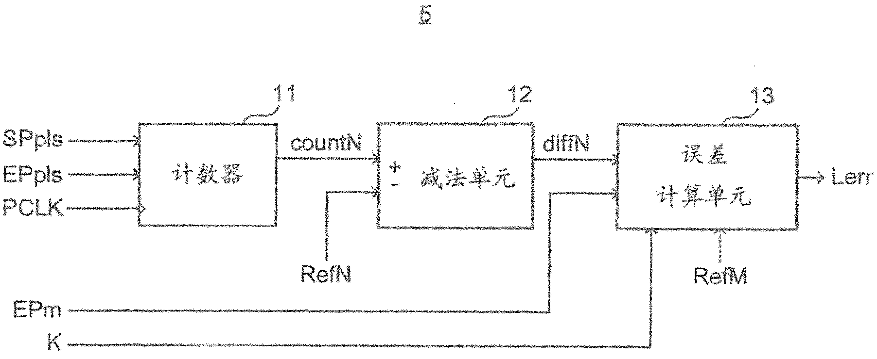
[0263] The pixel clock generation unit 118 includes a high frequency clock generation unit 51 , a first edge detection unit 52 , a second edge detection unit 53 , a counting unit 54 , a comparator 55 , a filter 6 , a frequency calculation unit 7 and a pixel clock output unit 58 .

[0264] The count unit 54 forms a pixel clock generation unit of the present invention, and the comparator 55 forms an error calculation unit of the present invention.

[0265] The high-frequency clock generation unit 51 multiplies the re...


PUM


Abstract

A pixel clock generator includes a frequency divider 4 that generates a pixel clock PCLK based on a high frequency clock VCLK; a comparator 5 that calculates an error Lerr in the time obtained by integrating a cycle of the pixel clock PCLK for a target number RefN from a time when synchronization signals SPSYNC and EPSYNC are detected; a filter 6; and a frequency calculating unit 7 that sets a frequency dividing value M of the frequency divider 4. The filter 6 and the frequency calculating unit 7 calculate an average of a frequency of the pixel clock PCLK based on the error Lerr, determine a reference error value from the error Lerr in N-cycles, calculate offset values of the frequencies of N pieces of pixel clocks PCLK based on a difference between the reference error value and the error Lerr, and calculate the frequency dividing value M based on a result obtained by adding the circularly selected offset values and the average of the frequency of the pixel clock PCLK.

Description

technical field [0001] The present invention relates to a pixel clock generator and an imaging device. More specifically, the present invention relates to a pixel clock generator used in laser printers, digital copiers, etc., and an image forming apparatus including the pixel clock generator. Background technique [0002] Figure 36 is a general schematic configuration of a conventional imaging device. Such as Figure 36 As shown, laser light output from a semiconductor laser unit 1009 is scanned by a rotating polygon mirror 1003, and forms a light spot on a photosensitive element 1001 as a medium to be scanned via a scanning lens 1002. By exposing the photosensitive member 1001, an electrostatic latent image is formed on the photosensitive member 1001. At this time, the photodetector 1004 detects laser light on each line. [0003] The phase synchronization circuit 1006 generates a pixel clock whose phase is synchronized with the detection signal of the photodetector 1004...

Claims


Application Information

Patent Timeline
Patent Type & Authority Applications(China)
IPC IPC(8): B41J2/44G02B26/12H04N1/113
CPCG06K15/1219H04N1/12H04N2201/04772G03G15/043H04N1/053H04N2201/0082H04N2201/0471H04N1/1135G02B26/127H04N2201/04786H04N2201/02439H04N2201/04794H04N2201/04784H04N2201/04732H04N2201/04744H04N1/04G02B26/10
Inventor 增井成博
Owner RICOH KK
Why Eureka
Try Eureka