
Packaging structure for system level fan-out wafer

A wafer packaging and system-level technology, applied in the direction of electrical components, electrical solid-state devices, circuits, etc., can solve problems such as single chip functions, and achieve the effect of high integration

Active Publication Date: 2011-08-24
NANTONG FUJITSU MICROELECTRONICS
View PDF5 Cites 22 Cited by
  • Summary
  • Abstract
  • Description
  • Claims
  • Application Information

AI Technical Summary

Problems solved by technology

[0004] The final product packaged and manufactured according to the above method has only a single chip function

Method used


Image

  • Packaging structure for system level fan-out wafer
  • Packaging structure for system level fan-out wafer
  • Packaging structure for system level fan-out wafer

Examples


Embodiment Construction

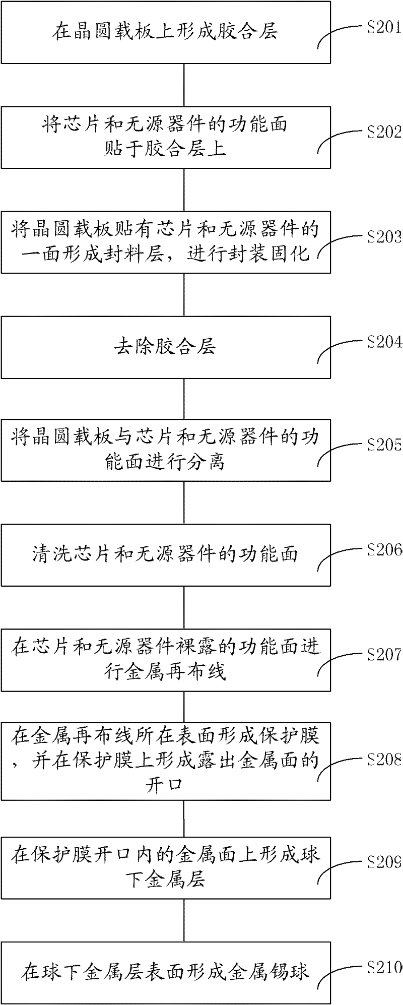
[0019] In the following description, numerous specific details are set forth in order to provide a thorough understanding of the present invention. However, the present invention can be implemented in many other ways different from those described here, and those skilled in the art can make similar extensions without violating the connotation of the present invention, so the present invention is not limited by the specific implementations disclosed below.

[0020] Secondly, the present invention is described in detail by means of schematic diagrams. When describing the embodiments of the present invention in detail, for convenience of explanation, the schematic diagrams are only examples, which should not limit the protection scope of the present invention.

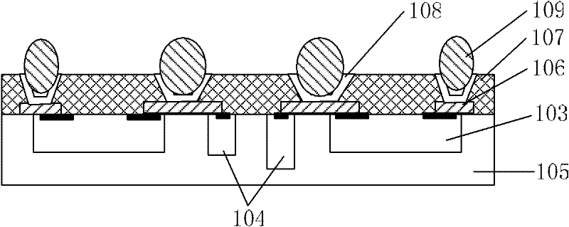
[0021] figure 1 It is a schematic cross-sectional view of the system-level fan-out wafer packaging structure of the present invention; the packaging structure includes: a sealing material layer 105, a chip 103 packaged an...


PUM


Abstract

The invention relates to a packaging structure for a system level fan-out wafer, and the packaging structure comprises a packaging material layer, a chip, a passive device, a metal re-wiring layer, a protective film layer, an under bump metal layer and metal solder balls, wherein the chip and the passive device are packaged and cured in the packaging material layer; the chip and the functional surface of the passive device are exposed on the surface of the packaging material layer; the metal re-wiring layer is formed on the surface of the packaging material layer and electrically connected with the chip and the functional surface of the passive device; the protective film layer is formed on the surface of the packaging material layer, and an opening for exposing the metal re-wiring layer is arranged on the protective film layer; the under bump metal layer which is connected with the metal re-wiring layer is formed in the opening; and the metal solder balls are formed on the under bump metal layer. The chip and the passive device in the packaging structure are integrated and then packaged together, thereby forming a packaging product with integral system function rather than the single chip function, having high degree of integration, further reducing resistance, inductance and other interference factors in the system, and better complying with the requirements of the trend of enabling the packaging of semiconductors to be light, thin, short and small.

Description

technical field [0001] The invention relates to semiconductor technology, in particular to a system-level fan-out wafer packaging structure. Background technique [0002] Wafer Level Packaging (WLP) technology is a technology that performs packaging and testing on the entire wafer and then cuts it to obtain a single finished chip. The size of the packaged chip is exactly the same as that of the bare chip. Wafer-level chip-scale packaging technology has completely subverted traditional packaging such as ceramic leadless chip carrier (Ceramic Leadless Chip Carrier) and organic leadless chip carrier (Organic Leadless Chip Carrier). Small, short, thin and low-cost requirements. The size of the chip packaged by the wafer-level chip size packaging technology has reached a high degree of miniaturization, and the cost of the chip is significantly reduced with the reduction of the chip size and the increase of the wafer size. Wafer-level chip-scale packaging technology is a technol...

Claims


Application Information

Patent Timeline
IPC IPC(8): H01L25/16H01L23/31H01L23/482H01L23/488
CPCH01L24/18H01L24/96H01L2224/24195H01L21/568H01L2224/04105H01L2224/12105H01L2224/19
Inventor 陶玉娟石磊高国华
Owner NANTONG FUJITSU MICROELECTRONICS
Learn More