Photosensitive chip encapsulation structure and manufacturing method thereof
A photosensitive chip and chip packaging technology, applied in radiation control devices and other directions, can solve the problems of insufficient light intensity and complicated processes
- Summary
- Abstract
- Description
- Claims
- Application Information
AI Technical Summary
Problems solved by technology
Method used
Image

Examples
Embodiment Construction
[0065] The features of the present invention can be clearly understood by referring to the drawings and detailed descriptions of the embodiments of the present application.
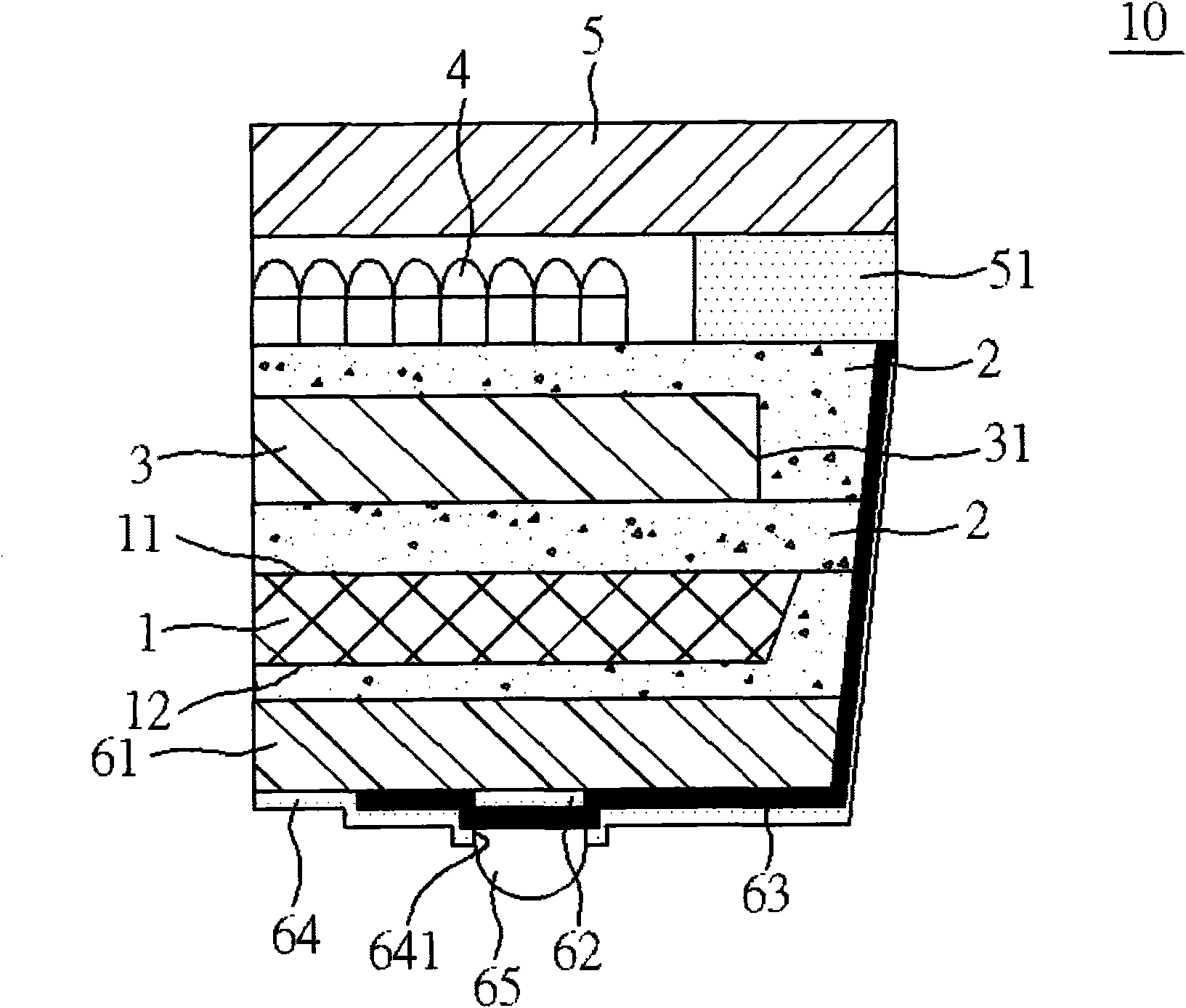
[0066] The "photosensitive chip packaging structure and its manufacturing method" of the present invention, the basic structure of the photosensitive chip packaging structure 10 is as follows figure 1 As shown, it contains at least:
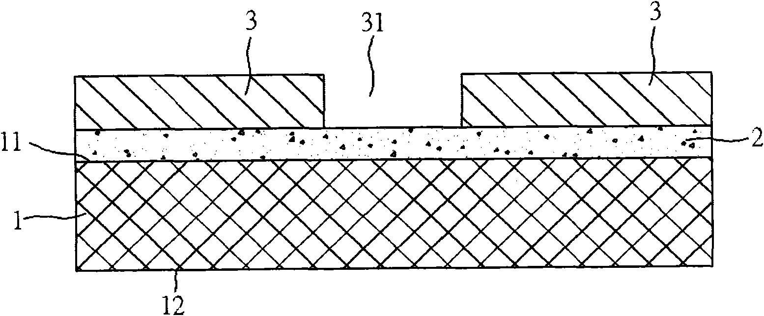
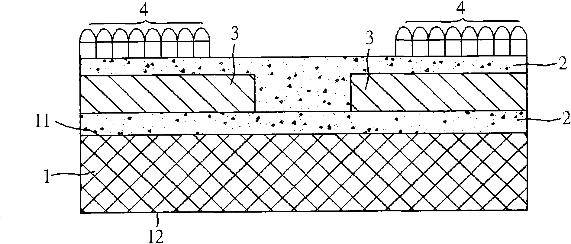
[0067] The wafer 1 is provided with first and second surfaces 11 , 12 , and the first surface 11 is bonded with several photosensitive chips 3 through the bonding layer 2 .
[0068] A plurality of photosensitive chips 3 with intervals 31 between each photosensitive chip 3 are arranged on the first surface 11 of the wafer 1 through a bonding layer 2 , and a color filter array 4 is arranged above each photosensitive chip 3 .
[0069] The color filter array 4 is respectively arranged above each photosensitive chip 3 by using the bonding layer 2 .
[0070] The glass substrate...
PUM
 Abstract
Description
Claims
Application Information