Defect correction device and defect tracking method

A technology of the defect and correction department, which is applied in the field of defect correction devices and defect tracking, and can solve problems such as increased number of steps, longer time, and complicated operations

Inactive Publication Date: 2011-09-21
OLYMPUS CORP
View PDF11 Cites 18 Cited by
  • Summary
  • Abstract
  • Description
  • Claims
  • Application Information

AI Technical Summary

Problems solved by technology

[0006] However, as described above, in the conventional defect correction technology, correcting a defect that cannot be completely captured by one shot requires at least two correction steps and the presence or absenc

Method used


Image

  • Defect correction device and defect tracking method
  • Defect correction device and defect tracking method
  • Defect correction device and defect tracking method

Examples


Embodiment approach 1

[0058] Next, the defect correction device, defect tracking method, and defect tracking program according to Embodiment 1 of the present invention will be described in detail using the drawings.

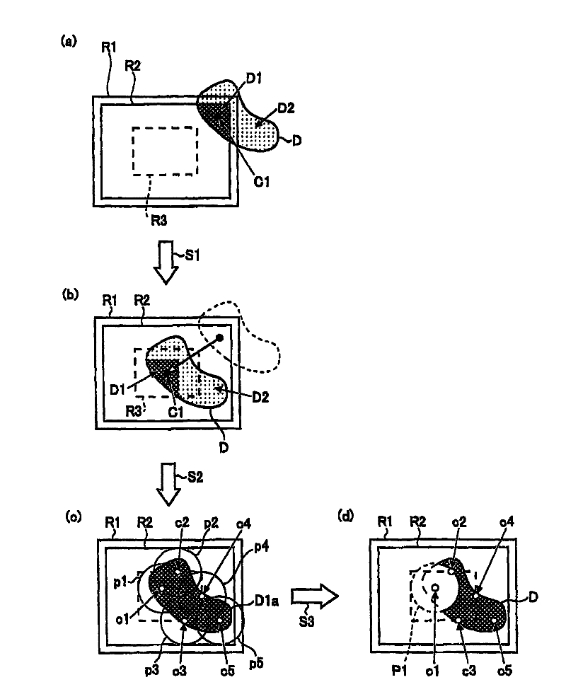
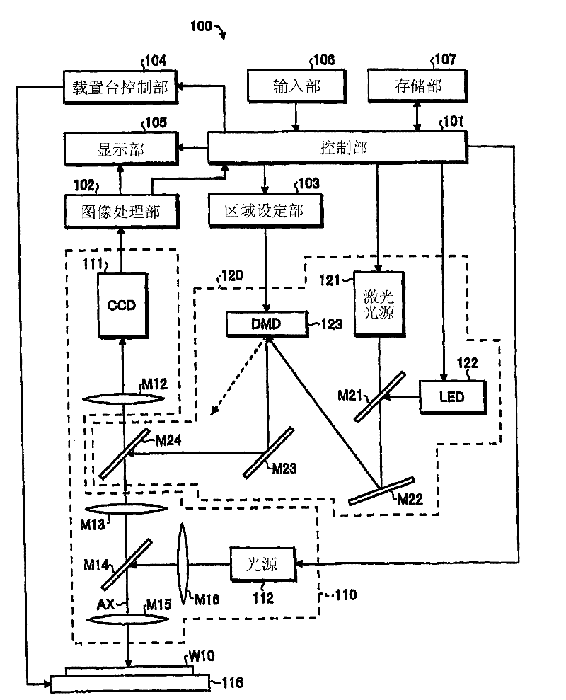
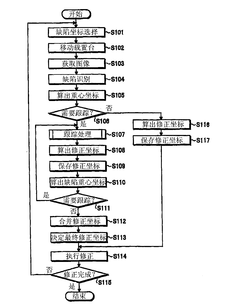
[0059] figure 1 is used to describe the defect correction device 100 incorporated in the first embodiment (refer to figure 2 Conceptual diagram of the outline of the defect tracking method of ). In this Embodiment 1, the coordinate of the defect specified by the external inspection means, such as an AOI (AUTOMATED OPTICAL INSPECTION: automatic optical inspection) system, is input to the defect correction apparatus 100, for example. This coordinate is called defect coordinate to distinguish it from other coordinates. Each defect is assigned a defect coordinate. In addition, in the following description, the coordinate refers to the surface of the workpiece or the upper surface of the stage with the reference position set on the upper surface of the stage on which the substrate (her...

Embodiment approach 2

[0091] Hereinafter, a defect correction device, a defect tracking method, and a defect tracking program according to Embodiment 2 of the present invention will be described in detail with reference to the drawings. In the above-described first embodiment, as the tracking process, the following case is taken as an example: the coordinates of the center of gravity C1 of the identification defect region D1 in the field of view region R1 are obtained, and the center of gravity C1 is dragged to the center of the field of view region R1. to track the defect D extending beyond the field of view area R1. In contrast, in the second embodiment, as the tracking process, correction coordinates are assigned to a portion previously identified as a defect in the field of view region R1 , and the correction coordinates are dragged to detect the defect D extending outside the field of view region R1 . Take the case of tracking as an example.

[0092] Figure 7 is used to describe the defect ...

Embodiment approach 3

[0110] Hereinafter, a defect correction apparatus, a defect tracking method, and a defect tracking program according to Embodiment 3 of the present invention will be described in detail with reference to the drawings. In the third embodiment, as the tracking process, a case where dragging the center coordinates (hereinafter referred to as side center coordinates) of line segments intersecting the four sides of the defect D and the field of view region R1 (corresponding to an image), respectively, is taken as an example. , to track the defect D extending beyond the field of view area R1.

[0111] Figure 10 is used to describe the defect correction device 100 incorporated in the third embodiment (see figure 2 ) conceptual diagram of the outline of the defect tracking method. In addition, in this Embodiment 3, the defect correction apparatus 100 is the same as the defect correction apparatus 100 of Embodiment 1 (refer to figure 2 )same.

[0112] In the defect tracking meth...


PUM


Abstract

The invention discloses a defect correction device and a defect tracking method. The defect correction device, which already comprises an image pickup part for obtaining an image after one part of an object substrate is amplified and a defect correction part for correcting the object substrate according to the image obtained by the image pickup part, comprises a judging part for judging whether the defect in the image obtained by the image pickup part extends outside of the image, a tracking part for tracking the part extending outside of the image when the defect extends outside of the image, and a setting part for setting more than one correction regions to the defect in the image obtained by the image pickup part. After the tracking part tracks the image, the setting part sets more than one correction regions to the defect in the image obtained by the image pickup part.

Description

technical field [0001] The present invention relates to a defect correcting device and a defect tracking method, and more particularly to a defect correcting device and a defect tracking method for correcting patterning errors (defects) generated during patterning processing of various substrates. Background technique [0002] Conventionally, liquid crystal displays (LCD: Liquid Crystal Display), PDP (Plasma Display Panel: Plasma Display Panel), organic EL (Electro Luminescence: Electroluminescence) displays, surface conduction electron emitting device displays (SED: Surface-conduction Electron In the manufacture of various substrates such as FPD (Flat Panel Display) substrates such as -emitterDisplay, semiconductor wafers, and printed circuit boards, in order to improve the product quality of various substrates, after each pattern formation process is performed, sequentially Check for pattern formation errors such as short circuits, poor connections, open circuits, and poor...

Claims


Application Information

Patent Timeline
IPC IPC(8): B23K26/00B23K26/03B23K26/04B23K26/06G01N21/956B23K26/064
Inventor 山崎隆一
Owner OLYMPUS CORP
Why Eureka
Try Eureka