Switching device driving unit and semiconductor apparatus

A technology for switching equipment and driving devices, which is applied in the direction of electronic switches, output power conversion devices, electrical components, etc.

Inactive Publication Date: 2011-10-05
PANASONIC CORP
View PDF1 Cites 21 Cited by
  • Summary
  • Abstract
  • Description
  • Claims
  • Application Information

AI Technical Summary

Problems solved by technology

In addition, in the case of a FET using a p-type region or a Schottky electrode for the gate, in a stable ON operation state, only the gate current of the VGS voltage for driving the drain current or the gate current for driving the collector is required. The base current of the current, when the constant voltage circuit of the above-mentioned switching device driving device operates, the gate current flowing into the switching device gate terminal becomes an unnecessary power loss in the switching device and the switching device driving device
This is also the case when bipolar transistors are used for switching devices

Method used


Image

  • Switching device driving unit and semiconductor apparatus
  • Switching device driving unit and semiconductor apparatus
  • Switching device driving unit and semiconductor apparatus

Examples


no. 1 Embodiment approach

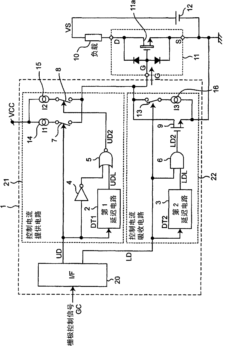
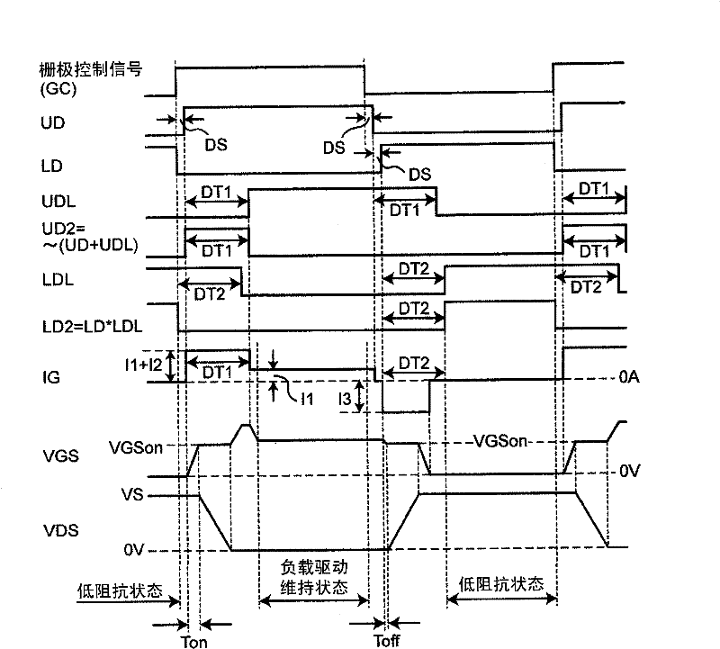
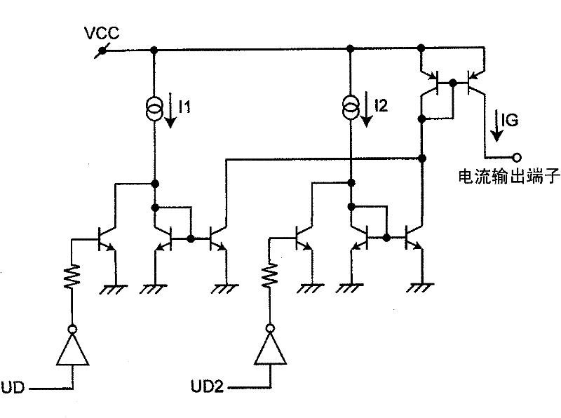
[0058] figure 1 A specific configuration block diagram showing the first embodiment of the switching device driving device and the semiconductor device according to the present invention. Below, use figure 1 The first embodiment of the switch gear drive device according to the present invention will be described.

[0059] The switching device driving device 1 for turning on / off (ON / OFF) driving (switching action) of the switching device 11 is configured to include: an I / F (interface) circuit 20, inputting a gate control signal (GC); controlling current Provide a circuit (control current source circuit) 21, input the signal (UD) from the I / F circuit 20, connected to the power supply side (VCC); and control current sink circuit (control current sink circuit) 22, input from the I / F circuit 20 The signal (LD) is connected to the ground side. The outputs of the control current supply circuit 21 and the control current sink circuit 22 are input to the gate terminal (G) of the switch...

no. 2 Embodiment approach

[0116] Figure 4 It is a specific configuration block diagram showing the second embodiment of the switching device driving device and the semiconductor device according to the present invention. Below, use Figure 4 The second embodiment of the switching device driving device and the semiconductor device according to the present invention will be described. In addition, in the description of the switching device driving device and the semiconductor device of the second embodiment, the same functions and components as those of the switching device driving device and the semiconductor device of the first embodiment described above are given the same reference numerals, and their description is omitted. .

[0117] The switching device driving device 30 for turning on / off driving (switching action) of the switching device 11 is configured to include: an I / F (interface) circuit 31 to which a gate control signal (GC) is input; and a control current supply circuit 40, Input the signal...


PUM


Abstract

The invention provides a switching device driving unit that, even in a case where a threshold voltage of a switching device is varied, can suppress variations in switching speed, and prevent a power loss caused by an unnecessary gate current in a constant ON operation state of the switching device, so that a desired slew rate can be easily set. A control current source circuit (21) sets to different values based on a first input driving signal (UD), in a driving current to be source-outputted to a gate or a base of the switching device (11), a current (I1+I2) in a stage of an initial ON operation of a switching operation of the switching device and a current (I1) in a stage after completion of the switching operation.

Description

Technical field [0001] The present invention relates to a switching device driving device and a semiconductor device for driving and controlling a switching device mounted in a semiconductor integrated circuit device, etc., and more particularly to a FET using a p-type region or Schottky electrode for the gate, or a bipolar transistor. A switching device drive device and a semiconductor device that perform drive control (switch drive) of a switching device through which gate current or base current flows when a bias voltage is applied to the gate or base. Background technique [0002] Image 6 It is a block diagram showing a conventional switchgear driving device disclosed in JP 2009-11049 A (Patent Document 1). [0003] Image 6 The conventional switching device driving device shown is a switching device driving device suitable for switching and driving a switching device whose gate terminal is a high impedance control terminal of an IGBT or MOS transistor. In this switching device...

Claims


Application Information

Patent Timeline
Patent Type & Authority Applications(China)
IPC IPC(8): H02M1/08
CPCH03K17/164H02M1/08H03K17/145
Inventor 玉冈修二
Owner PANASONIC CORP
Why Eureka
Try Eureka